SLPS732B june 2021 – april 2023 JFE150
PRODUCTION DATA
- 1 Features
- 2 Applications
- 3 Description
- 4 Revision History
- 5 Pin Configuration and Functions
- 6 Specifications
- 7 Parameter Measurement Information
- 8 Detailed Description
- 9 Application and Implementation
- 10Device and Documentation Support
- 11Mechanical, Packaging, and Orderable Information
Package Options
Mechanical Data (Package|Pins)
Thermal pad, mechanical data (Package|Pins)
Orderable Information
3 Description
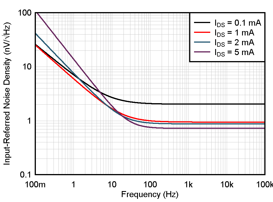
The JFE150 is a Burr-Brown™ discrete JFET built using Texas Instruments' modern, high-performance, analog bipolar process. The JFE150 features performance not previously available in older discrete JFET technologies. The JFE150 offers the maximum possible noise-to-power efficiency and flexibility, where the quiescent current can be set by the user and yields excellent noise performance for currents from 50 μA to 20 mA. When biased at 5 mA, the device yields 0.8 nV/√Hz of input-referred noise, giving ultra-low noise performance with extremely high input impedance (> 1 TΩ). The JFE150 also features integrated diodes connected to separate clamp nodes to provide protection without the addition of high-leakage, nonlinear, external diodes.
The JFE150 can withstand a high drain-to-source voltage of 40 V, as well as gate-to-source and gate-to-drain voltages down to –40 V. The temperature range is specified from –40°C to +125°C. The device is offered in 5-pin SOT-23 and SC70 packages.
| PART NUMBER | PACKAGE(1) | BODY SIZE (NOM) |
|---|---|---|
| JFE150 | DBV (SOT-23, 5) | 2.90 mm × 1.60 mm |
| DCK (SC70, 5) | 2.00 mm × 1.25 mm |
| PARAMETER | VALUE | |
|---|---|---|
| VGSS | Gate-to-source breakdown voltage | –40 V |
| VDSS | Drain-to-source breakdown voltage | ±40 V |
| CISS | Input capacitance | 24 pF |
| TJ | Junction temperature | –40°C to +125°C |
| IDSS | Drain-to-source saturation current | 35 mA |
 Functional Block Diagram
 Ultra-Low Input Voltage Noise