SNOSD15B December 2016 – April 2017 LDC2112 , LDC2114
PRODUCTION DATA.
- 1 Features
- 2 Applications
- 3 Description
- 4 Revision History
- 5 Pin Configuration and Functions
- 6 Specifications
-
7 Detailed Description
- 7.1 Overview
- 7.2 Functional Block Diagram
- 7.3 Feature Description
- 7.4 Device Functional Modes
- 7.5 Register Maps
-
8 Application and Implementation
- 8.1
Application Information
- 8.1.1 Theory of Operation
- 8.1.2 Designing Sensor Parameters
- 8.1.3 Setting COM Pin Capacitor
- 8.1.4 Defining Power-On Timing
- 8.1.5 Configuring Button Scan Rate
- 8.1.6 Programming Button Sampling Window
- 8.1.7 Scaling Frequency Counter Output
- 8.1.8 Setting Button Triggering Threshold
- 8.1.9 Tracking Baseline
- 8.1.10 Mitigating False Button Detections
- 8.1.11 Reporting Interrupts for Button Presses and Error Conditions
- 8.1.12 Estimating Supply Current
- 8.2 Typical Application
- 8.1
Application Information
- 9 Power Supply Recommendations
- 10Layout
- 11Device and Documentation Support
- 12Mechanical, Packaging, and Orderable Information
Package Options
Mechanical Data (Package|Pins)
Thermal pad, mechanical data (Package|Pins)
Orderable Information
8 Application and Implementation
NOTE
Information in the following applications sections is not part of the TI component specification, and TI does not warrant its accuracy or completeness. TI’s customers are responsible for determining suitability of components for their purposes. Customers should validate and test their design implementation to confirm system functionality.
8.1 Application Information
The LDC2112/LDC2114 supports multiple buttons. Each button can be configured in various ways for optimal operation.
8.1.1 Theory of Operation
An AC current flowing through an inductor will generate an AC magnetic field. If a conductive material, such as a metal object, is in close proximity to the inductor, the magnetic field will induce circulating eddy currents on the surface of the conductor. The eddy currents are a function of the distance, size, and composition of the conductor. If the conductor is deflected toward the inductor as shown in Figure 17, more eddy currents will be generated.
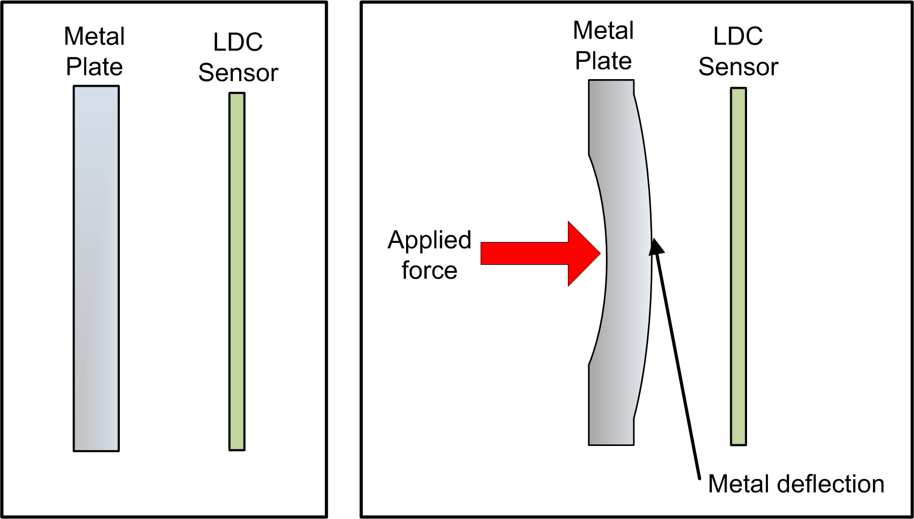 Figure 17. Metal Deflection
The eddy currents create their own magnetic field, which opposes the original field generated by the inductor. This effect reduces the effective inductance of the system, resulting in an increase in sensor frequency. Figure 18 shows the inductance and frequency response of an example sensor with a diameter of 14 mm. As the sensitivity of an inductive sensor increases with closer targets, the conductive plate should be placed quite close to the sensor—typically 10% of the sensor diameter for circular coils. For rectangular or race-track-shaped coils, the target to sensor distance should typically be less than 10% of the shorter side of the coil.
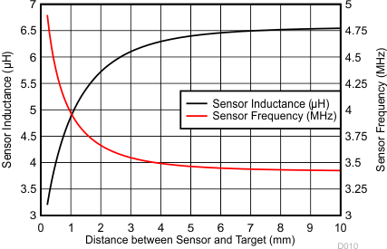 Figure 18. Sensor Inductance and Frequency vs Target Distance. Sensor Diameter = 14 mm
The output DATAn registers (Addresses 0x02 through 0x09) of the LDC2112/LDC2114 contain the processed values of the changes in sensor frequencies.
8.1.2 Designing Sensor Parameters
Each inductive touch button uses an LC resonator sensor, as illustrated in Figure 19, where L is the inductor, C is the capacitor, and RS is the AC series resistance of the sensor at the frequency of operation. The key parameters of the LC sensor include frequency, effective parallel resistance RP, and quality factor Q. These parameters must be within the ranges as specified in the Sensor section of the Electrical Characteristics table. Note that the effective RP and Q changes when the conductive target is in place.
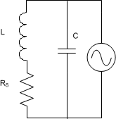 Figure 19. LC Resonator
The LC sensor frequency, as defined by the equation below, must be between 1 MHz and 30 MHz.

The sensor quality factor, as defined by the equation below, must be between 5 and 30.

The series resistance can be represented as an equivalent parallel resistance, RP, which is given by

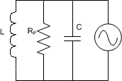 Figure 20. Equivalent Parallel Circuit
RP can be viewed as the load on the sensor driver. This load corresponds to the current drive needed to maintain the oscillation amplitude. RP must be between 350 Ω and 10 kΩ.
In summary, the LDC2112/LDC2114 requires that the sensor parameters are within the following ranges when the conductive target is present:
- 1 MHz ≤ fSENSOR ≤ 30 MHz
- 5 ≤ Q ≤ 30
- 350 Ω ≤ RP ≤ 10 kΩ
8.1.3 Setting COM Pin Capacitor
The COM pin requires a bypass capacitor to ground. The capacitor should be a low ESL, low ESR type. CCOM must be sized so that the following relationship is valid for all channels.
The value of QSENSORn when the sensor is at the minimum target distance should be used. The maximum acceptable value for CCOM is 20 nF. The CCOM range for a particular sensor configuration can be obtained with the Spiral_Inductor_Designer tab of the LDC Calculations Tool.
8.1.4 Defining Power-On Timing
The low power architecture of the LDC2112/LDC2114 makes it possible for the device to be active all the time. When not being used, the LDC2112/LDC2114 can operate in Low Power Mode with a single standby power button, which typically consumes less than 10 µA. If additional power-saving is desired, or in the rare event where a power-on reset becomes necessary (see I2C Interface), the output data will become ready after 50 ms startup time, about 1 ms optional register loading time, and two sampling windows for all active channels. The power-on timing of the LDC2112/LDC2114 is illustrated in Figure 21 below.
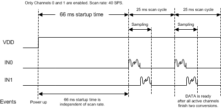 Figure 21. Power-On Timing
8.1.5 Configuring Button Scan Rate
The LDC2112/LDC2114 periodically samples all active channels at the selected scan rate. The device can operate at eight different scan rates to meet various power consumption requirements, where a lower scan rate achieves lower power consumption. In Normal Power Mode, the scan rate can be programmed to 80, 40, 20, or 10 SPS through Register NP_SCAN_RATE (Address 0x0D). In Low Power Mode, the scan rate can be programmed to 5, 2.5, 1.25, or 0.625 SPS through Register LP_SCAN_RATE (Address 0x0F). The mode is selected by setting the LPWRB pin to VDD (Normal Power) or ground (Low Power). In either mode, each button can be independently enabled through a bit in Register EN (Address 0x0C). For typical distribution of the scan rates, refer to Figure 9.
Table 42. Button Scan Rates
| SCAN RATE (SPS) | LPSR (0x0F) SETTING | NPSR (0x0D) SETTING | LPWRB PIN SETTING |
|---|---|---|---|
| 0.625 | b11 | Not Applicable | Ground |
| 1.25 | b10 | Not Applicable | Ground |
| 2.5 | b01 | Not Applicable | Ground |
| 5 | b00 | Not Applicable | Ground |
| 10 | Not Applicable | b11 | VDD |
| 20 | Not Applicable | b10 | VDD |
| 40 | Not Applicable | b01 | VDD |
| 80 | Not Applicable | b00 | VDD |
8.1.6 Programming Button Sampling Window
The button sampling window is the actual duration per scan cycle for active data sampling of the sensor frequency. It is programmed with the exponential parameter, LCDIV, in Register LC_DIVIDER (Address 0x17), and the individual linear sensor cycle counter SENCYCn (n = 0, 1, 2, or 3) in Registers SENSORn_CONFIG (n = 0, 1, 2, or 3, Addresses 0x20, 0x22, 0x24, 0x26). For most touch button applications, the button sampling window should be set to between 1 ms and 8 ms. The recommended minimum sensor conversion time is 1 ms. Longer conversion time can be used to achieve better signal-to-noise ratio if needed. If multiple channels are enabled, the active channels will sample sequentially, as illustrated in Figure 22.
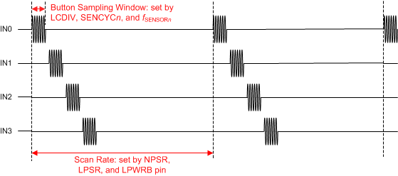 Figure 22. Configurable Scan Rate and Button Sampling Window
The LDC2112/LDC2114 is designed to work with LC resonator sensors with oscillation frequencies ranging from 1 MHz to 30 MHz. The exact definition of the button sampling window is given by the equation below.

where
- tSAMPLE is the button sampling window in µs,
- SENCYCn and LCDIV are the linear and exponential scalers that set the number of sensor oscillation cycles, and
- fSENSORn is the sensor frequency in MHz.
In the equation above, LCDIV (0 to 7, default 3) is the exponential LC divider that sets the approximate ranges for all channels, and SENCYCn (0 to 31, default 4) is the linear sensor cycle scaler that fine-tunes each individual channel. Together they set the number of sensor oscillation cycles used to determine the button sampling window.
For example, if the LC sensor frequency is 9.2 MHz, and it is desirable to get 1 ms button sampling window, then this can be achieved by setting SENCYCn = 17 and LCDIV = 2.
Alternatively, from the button sampling window and sensor frequency, the LCDIV can be read off from Figure 23. For example, 1 ms button sampling window and 9.2 MHz sensor frequency intersect at the region where LCDIV = 2. Then SENCYCn can be calculated accordingly.
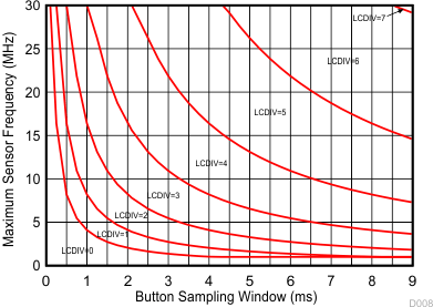 Figure 23. LCDIV as a Function of Sensor Frequency and Button Sampling Window
8.1.7 Scaling Frequency Counter Output
The LDC2112/LDC2114 requires this internal frequency counter scaler to be set based on the button sampling window to avoid data overflow. The scaler in Register CNTSC (Address 0x1E) must be set by the following formula:

where
- CNTSCn is the internal frequency counter scaler,
- SENCYCn and LCDIV are the linear and exponential scalers that set the number of sensor oscillation cycles, and
- fSENSORn is the sensor frequency in MHz.
8.1.8 Setting Button Triggering Threshold
Every material shows some hysteresis when it deforms then returns to the original state. The amount of hysteresis is a function of material properties and physical parameters, such as size and thickness. This feature modifies the hysteresis of the button signal threshold according to different materials and various button shapes and sizes. Hysteresis can be programmed in Register HYST (Address 0x18). By default, the button triggering hysteresis is set to 32. The nominal button triggering threshold is 128. With hysteresis, the effective on-threshold is 128 + 32 = 160. This means if the DATAn (n = 0, 1, 2, or 3) reaches 160, the LDC considers that as a button press. When the DATAn decreases to 128 – 32 = 96, the LDC considers the button to be released.


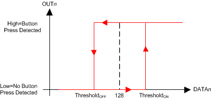 Figure 24. Button Triggering Threshold with Hysteresis. Output Polarity: Active High
8.1.9 Tracking Baseline
The LDC2112/LDC2114 automatically tracks slow changes in the baseline signal and compensates for environmental drifts and variations. In Normal Power Mode, the effective baseline increment per scan cycle (BINCNP) can be determined by Equation 9:

where
- NPBI is the Normal Power Baseline Increment index that can be configured in Register NP_BASE_INC (Address 0x15).
In Low Power Mode, the effective baseline increment per scan cycle (BINCLP) can be determined by Equation 10:

where
- LPBI the Low Power Baseline Increment index that can be configured in Register LP_BASE_INC (Address 0x13).
As a result of baseline tracking, a button press with a constant force only lasts for a finite amount of time. The duration of a button press is defined by Equation 11 (DATAn > ThresholdON).

where
- Duration of Button Press is the number of scan cycles that the channel is asserted,
- DATAn is the button signal at the beginning of a press, and
- BINC is the baseline increment per scan cycle.
The baseline tracking for a particular channel can be paused when the channel output is asserted. This is achieved by setting the corresponding BTPAUSE bit in Register BTPAUSE_MAXWIN (Address 0x16) to b1.
If DATAn is negative, the tracking speed will be scaled by the fast tracking factor as specified in Registers FTF0 (Address 0x25), FTF1_2 (Address 0x28), or FTF3 (Address 0x2B). The scaling factors for various FTFn settings are shown in Table 43.
Table 43. Fast Tracking Factor Settings
| FTFn Setting | Fast Tracking Factor |
|---|---|
| b00 | 1 |
| b01 | 4 |
| b10 | 8 |
| b11 | 16 |
8.1.10 Mitigating False Button Detections
The LDC2112/LDC2114 offers several algorithms that can mitigate false button detections due to mechanical non-idealities associated with groups of buttons. These are listed below.
8.1.10.1 Eliminating Common-Mode Change (Anti-Common)
This algorithm eliminates false detection when a user presses the middle of two or more buttons, which could lead to a common-mode response on multiple buttons. All the buttons can be individually enabled to have this feature by programming Register COMMON_DEFORM (Address 0x1A).
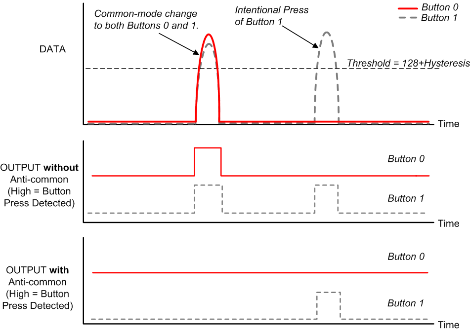 Figure 26. Illustration of the Anti-Common Feature
8.1.10.2 Resolving Simultaneous Button Presses (Max-Win)
This algorithm enables the system to select the button pressed with maximum force when multiple buttons are pressed at the same time. This could happen when two buttons are physically very close to each other, and pressing one causes a residual reaction on the other. Buttons can be individually enabled to join the “max-win” group by configuring Register BTPAUSE_MAXWIN (Address 0x16).
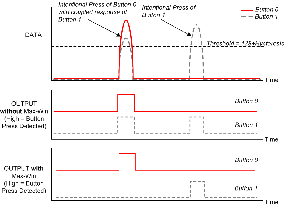 Figure 27. Illustration of the Max-Win Feature
8.1.10.3 Overcoming Case Twisting (Anti-Twist)
The anti-twist algorithm reduces the likelihood of false detection when the case is twisted, which could cause unintended mechanical activation of the buttons, or an opposite reaction in two adjacent buttons. When this algorithm is enabled, detection of button presses is suppressed if any button’s output data is negative by a configurable threshold. The anti-twist algorithm can be enabled by configuring Register TWIST (Address 0x19).
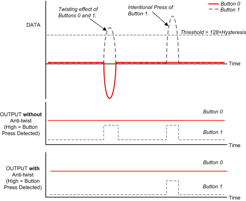 Figure 28. Illustration of the Anti-Twist Feature
8.1.10.4 Mitigating Metal Deformation (Anti-Deform)
This function filters changes due to metal deformation in the vicinity of one or more buttons. Such metal deformation can be accidentally caused by pressing a neighboring button that does not have sufficient mechanical isolation. The user can specify which buttons to join the anti-deform group by configuring Register COMMON_DEFORM (Address 0x1A).
8.1.11 Reporting Interrupts for Button Presses and Error Conditions
INTB, the LDC2112/LDC2114 interrupt pin, is asserted when a button press or an error condition occurs. The default polarity is active low and can be configured through Register INTPOL (Address 0x11).
Figure 29 shows the LDC2112/LDC2114 response to a single button press on Channel 0. At the end of the button sampling window following a press of Button 0, the OUT0 pin and INTB pin are asserted. The OUT_STATUS bit changes from 0 to 1, and remains so until a read of the STATUS register clears it. The OUTn (n = 0, 1, 2, or 3) and INTB pins are asserted until the end of the button sampling window following the release of the button.
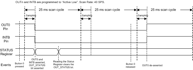 Figure 29. Timing Diagram of a Single Button Press
Figure 30 shows the LDC2112/LDC2114 response to multiple button presses. In this example, after Button 0 is pressed, the OUT0 pin is asserted. After that, Button 1 is also pressed, following which Button 0 is released. The OUT0 pin is de-asserted and OUT1 pin asserted at the end of the next button sampling window. The INTB pin remains continuously asserted as long as at least one of the buttons is pressed. The OUT_STATUS bit only changes from 0 to 1 after the first button assertion.
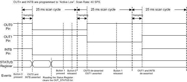 Figure 30. Timing Diagram of Multiple Button Presses
The INTB pin also reports any error event. If an error occurs, the INTB pin is asserted and the error is reported in the STATUS register (Address 0x00). Refer to Register STATUS (Address 0x00) for possible error events.
8.1.12 Estimating Supply Current
When the LDC2112/LDC2114 is active (in either Normal Power Mode or Low Power Mode), its current can be characterized by Equation 13:

where
- IACTIVEn is the supply current in mA during active sampling,
- RPn is the sensor parallel resonant impedance in kΩ,
- fSENSORn is the sensor frequency in MHz, and
- n is the channel index, i.e. n = 0 or 1 for LDC2112; n = 0, 1, 2, or 3 for LDC2114.
The LDC2112/LDC2114 is only actively sampling the enabled channels during a fraction of the scan window. So the average supply current is:

where
- IDD is the average supply current in mA,
- tSCAN is the scan window (set by the scan rate) in ms,
- IACTIVEn is the supply current when the device is active as defined by Equation 13, and
- tSAMPLE is the button sampling window in ms.
8.2 Typical Application
8.2.1 Touch Button Design
The low power architecture of LDC2112/LDC2114 makes them suitable for driving button sensors in consumer electronics, such as mobile phones. Most mobile phones today have three buttons along the edges, namely the power button, volume up, and volume down. The LDC2112 can support two buttons, and LDC2114 can support four.
On a typical smartphone, the two volume buttons are next to each other, so they may be susceptible to false detections such as simultaneous button presses. To prevent such mis-triggers, they can be grouped together to take advantage of the various features that mitigate false detections as explained in Mitigating False Button Detections. For example, if Max-win is applied to the two volume buttons, only the one with the greater force will be triggered.
The inductive touch solution does not require any mechanical cutouts at the button locations. This can support reduced manufacturing cost for the phone case and enhance the case’s resistance to moisture, dust, and dirt. This is a great advantage compared to mechanical buttons in the market today.
8.2.1.1 Design Requirements
The sensor parameters, including frequency, RP, and Q factor have to be within the design space of the LDC2112/LDC2114 as specified in Electrical Characteristics.
8.2.1.2 Detailed Design Procedure
The LDC2112/LDC2114 is a multi-channel device. The italic n in the parameters below refers to the channel index, i.e., n = 0 or 1 for LDC2112, and n = 0, 1, 2, or 3 for LDC2114.
1. Select system-based options:
- Select Normal or Low Power Mode of operation by setting the LPWRB pin to VDD or Ground, respectively. Configure the enable bits for all channels in Register EN (Address 0x0C).
- Select the polarities of OUTn and INTB pins by configuring Register OPOL_DPOL (Address 0x1C) and Register INTPOL (Address 0x11).
- Configure the sensor frequency setting in Registers SENSORn_CONFIG (Addresses 0x20, 0x22, 0x24, 0x26).
2. Choose the sampling rate (80, 40, 20, 10, 5, 2.5, 1.25, or 0.625 SPS) based on system power consumption requirement, and configure Register NP_SCAN_RATE (Address 0x0D) or Register LP_SCAN_RATE (Address 0x0F).
3. Choose the button sampling window based on power consumption and noise requirements (recommended: 1 ms to 8 ms). While a longer button sampling window provides better noise performance, 1 ms is typically sufficient for most applications. Set SENCYCn and LCDIV in Registers SENSORn_CONFIG (Addresses 0x20, 0x22, 0x24, 0x26) and Register LC_DIVIDER (Address 0x17) in the following steps:
- Calculate LCDIV = ceiling (log2 (fSENSORn × tSAMPLEn) – 12), where fSENSORn is the sensor frequency in MHz, tSAMPLEn is the button sampling window in µs
- If LCDIV < 0, set it to 0
- Adjust SENCYCn to get desired tSAMPLEn according to tSAMPLEn = 128 × (SENCYCn + 1) × 2LCDIV / fSENSORn
4. Calibrate gain in the appropriate Registers GAINn (Addresses 0x0E, 0x10, 0x12, 0x14). The gain setting can be used to tune the sensitivity of the touch button. GAINn is a 6-bit field with 64 different gain levels corresponding to normalized gains between 1 and 232. A good mechanical and sensor design typically requires a gain level of around 32 to 50, corresponding to relative gains of 16 to 76 (normalized to gain level of 0). Use the following sequence to determine the appropriate gain for each button:
- Apply minimum desired force to the button.
- Read initial DATAn value after the button press. Note that the baseline tracking will affect this value.
- Calculate gain factor needed to increase DATAn to the programmed threshold (default is 160).
- Look up the Gain Table to find the required gain setting.
5. Enable special features to mitigate button interference if there is any. Registers BTPAUSE_MAXWIN, TWIST, COMMON_DEFORM (Addresses 0x16, 0x19, 0x1A).
For more information on inductive touch system design, including mechanical design and sensor electrical design, refer to Inductive Touch System Design Guide.
8.2.1.3 Application Curves
Figure 31 shows a sequence of button presses of 150 grams force, two presses to Channel 0, then two presses to Channel 1. Each button press response is greater than the threshold.
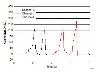 Figure 31. Conversion DATA vs Time for Channels 0 and 1