SNOSDI7 December 2023 LDC5071-Q1
PRODUCTION DATA
- 1
- 1 Features
- 2 Applications
- 3 Description
- 4 Pin Configuration and Functions
- 5 Specifications
- 6 Detailed Description
- 7 Application and Implementation
- 8 Device and Documentation Support
- 9 Revision History
- 10Mechanical, Packaging, and Orderable Information
Package Options
Mechanical Data (Package|Pins)
- PW|16
Thermal pad, mechanical data (Package|Pins)
Orderable Information
6.1 Overview
The LDC5071-Q1 is an inductive position sensor front-end IC for use in automotive and industrial applications. The sensor typically consists of an excitation coil and a set of two receiver coils, all drawn on the same PCB. The sensor also has a metal target which is typically printed on another PCB. The coil PCB is mounted in a fixed position on the motor and the metal target is mounted on a rotating shaft. The device excites the excitation coil, which then couples to the receiver coils. The amount of coupling from the excitation to receiver coils depends on the relative position of the metal target to the receiver coils and also on the air gap between the coil PCB and the target. The LDC5071-Q1 has an LC oscillator driver that can drive an excitation coil with a constant amplitude and supports a wide range of LC combinations.
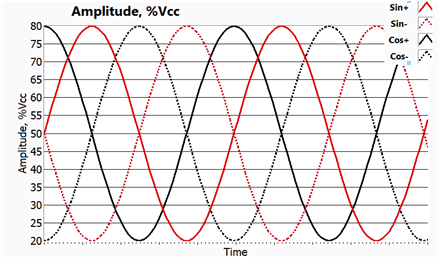
Two receiver coils are placed such that the LDC5071-Q1 outputs are shifted by 90°. These Sine and Cosine outputs are ratiometric to each other and can be used to calculate the angle at any given instant. The LDC5071-Q1 receiver filters out the out-of-band noise, demodulates, and amplifies the signal. The device has a gain block that can be either set manually or in automatic mode. In automatic mode, the LDC5071-Q1 will regulate output amplitude to a fixed band, which can remove sensor variability such as the lifetime variation of air gap. The device has two differential output drivers that can drive a wide range of capacitive loads. Typically these are digitized by an ADC of an MCU for further angle calculation, for motor control, or for linear position information extraction.
 Figure 6-1 LDC5071-Q1 Typical Output
The LDC5071-Q1 implements a pin-level built-in self-test at power up to check for sensor pins open, shorts to supplies, and short between the coils. The device also has analog and digital built-in self-test to test internal safety mechanisms.