SNOSBH0D May 2000 – November 2015 LF156 , LF256 , LF356
PRODUCTION DATA.
- 1 Features
- 2 Applications
- 3 Description
- 4 Revision History
- 5 Pin Configuration and Functions
-
6 Specifications
- 6.1 Absolute Maximum Ratings
- 6.2 ESD Ratings
- 6.3 Recommended Operating Conditions
- 6.4 Thermal Information
- 6.5 AC Electrical Characteristics, TA = TJ = 25°C, VS = ±15 V
- 6.6 DC Electrical Characteristics, TA = TJ = 25°C, VS = ±15 V
- 6.7 DC Electrical Characteristics
- 6.8 Power Dissipation Ratings
- 6.9 Typical Characteristics
- 7 Detailed Description
- 8 Application and Implementation
- 9 Power Supply Recommendations
- 10Layout
- 11Device and Documentation Support
- 12Mechanical, Packaging, and Orderable Information
Package Options
Mechanical Data (Package|Pins)
- LMC|8
Thermal pad, mechanical data (Package|Pins)
Orderable Information
7 Detailed Description
7.1 Overview
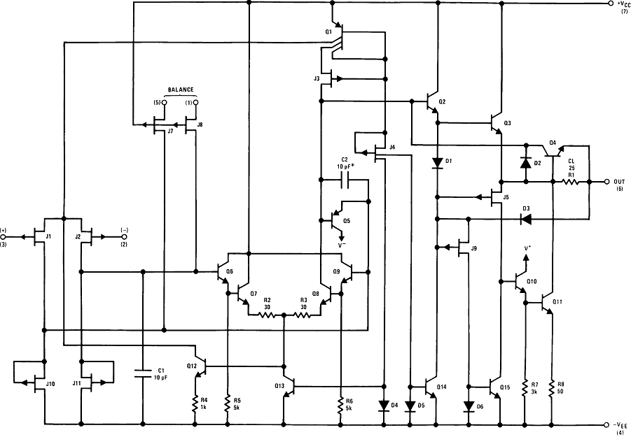
These are the first monolithic JFET input operational amplifiers to incorporate well matched, high voltage JFETs on the same chip with standard bipolar transistors (BI-FET Technology). These amplifiers feature low input bias and offset currents, as well as low offset voltage and offset voltage drift, coupled with offset adjust which does not degrade drift or common-mode rejection. These devices can replace expensive hybrid and module FET operational amplifiers. Designed for low voltage and current noise and a low 1/f noise corner, these devices are excellent for low noise applications using either high or low source impedance.
7.2 Functional Block Diagram

7.3 Feature Description
7.3.1 Large Differential Input Voltage
These are operational amplifiers with JFET input devices. These JFETs have large reverse breakdown voltages from gate to source and drain eliminating the need for clamps across the inputs. Therefore large differential input voltages can easily be accommodated without a large increase in input current. The maximum differential input voltage is independent of the supply voltages. However, neither of the input voltages should be allowed to exceed the negative supply as this will cause large currents to flow which can result in a destroyed unit.
7.3.2 Large Common-Mode Input Voltage
These amplifiers will operate with the common-mode input voltage equal to the positive supply. In fact, the common-mode voltage can exceed the positive supply by approximately 100 mV independent of supply voltage and over the full operating temperature range. The positive supply can therefore be used as a reference on an input as, for example, in a supply current monitor and/or limiter.
7.4 Device Functional Modes
The LFx5x has a single functional mode and operates according to the conditions listed in the Recommended Operating Conditions.