SNVS037H September 1999 – March 2024 LM1084
PRODUCTION DATA
- 1
- 1 Features
- 2 Applications
- 3 Description
- 4 Pin Configuration and Functions
- 5 Specifications
- 6 Detailed Description
-
7 Application and Implementation
- 7.1 Application Information
- 7.2
Typical Applications
- 7.2.1 1.2-V to 15-V Adjustable Regulator
- 7.2.2 Adjustable at 5 V
- 7.2.3 5-V Regulator With Shutdown
- 7.2.4 Battery Charger
- 7.2.5 Adjustable Fixed Regulator
- 7.2.6 Regulator with Reference
- 7.2.7 High Current Lamp Driver Protection
- 7.2.8 Battery Backup Regulated Supply
- 7.2.9 Ripple Rejection Enhancement
- 7.2.10 Automatic Light Control
- 7.2.11 Generating Negative Supply Voltage
- 7.2.12 Remote Sensing
- 7.3 Power Supply Recommendations
- 7.4 Layout
- 8 Device and Documentation Support
- 9 Revision History
- 10Mechanical, Packaging, and Orderable Information
Package Options
Mechanical Data (Package|Pins)
Thermal pad, mechanical data (Package|Pins)
- KTT|3
Orderable Information
6.3.2 Load Regulation
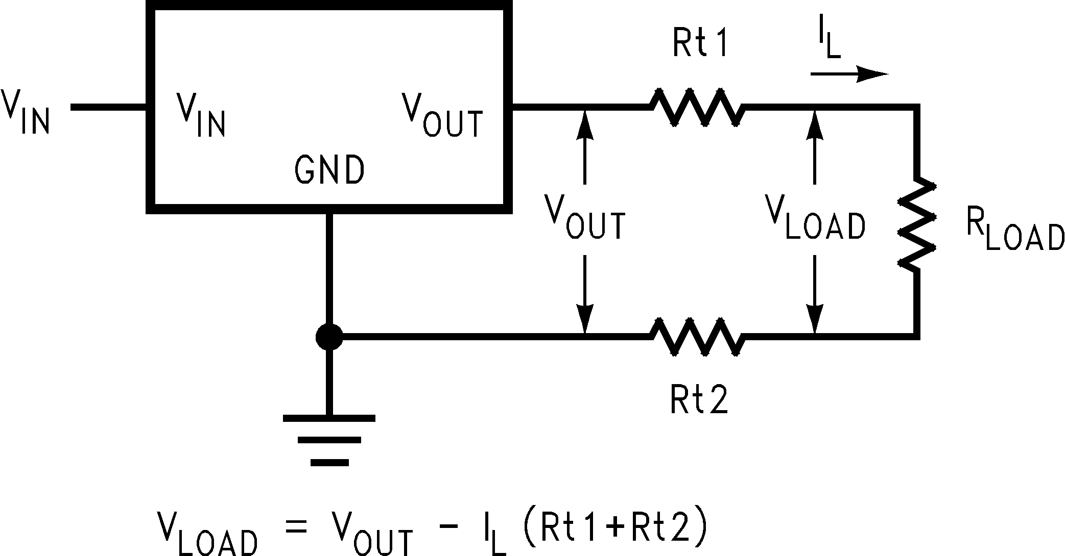
The LM1084 regulates the voltage that appears between its output and ground pins, or between its output and adjust pins. In some cases, line resistances can introduce errors to the voltage across the load. To obtain the best load regulation, a few precautions are needed.
Figure 6-2 shows a typical application using a fixed output regulator. Rt1 and Rt2 are the line resistances. VLOAD is less than the VOUT by the sum of the voltage drops along the line resistances. In this case, the load regulation seen at the RLOAD would be degraded from the data sheet specification. To improve this, the load should be tied directly to the output pin on the positive side and directly tied to the ground pin on the negative side.
 Figure 6-2 Typical Application Using Fixed Output Regulator
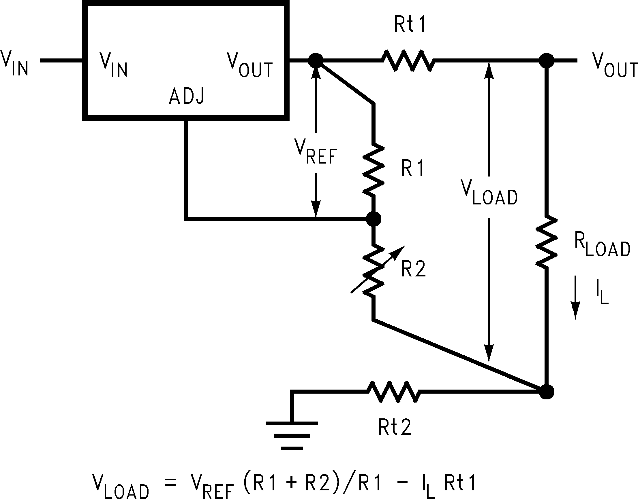
When the adjustable regulator is used (Figure 6-3), the best performance is obtained with the positive side of the resistor R1 tied directly to the output pin of the regulator rather than near the load. This eliminates line drops from appearing effectively in series with the reference and degrading regulation. For example, a 5-V regulator with 0.05Ω resistance between the regulator and load will have a load regulation due to line resistance of 0.05Ω × IL. If R1 (= 125Ω) is connected near the load the effective line resistance will be 0.05Ω (1 + R2/R1) or in this case, it is 4 times worse. In addition, the ground side of the resistor R2 can be returned near the ground of the load to provide remote ground sensing and improve load regulation.
 Figure 6-3 Best Load Regulation Using Adjustable Output Regulator