SNVSC12 April 2021 LM117QML-SP
PRODUCTION DATA
- 1 Features
- 2 Applications
- 3 Description
- 4 Revision History
- 5 Device Comparison Table
- 6 Pin Configurations and Functions
-
7 Specifications
- 7.1 Absolute Maximum Ratings
- 7.2 ESD Ratings
- 7.3 Recommended Operating Conditions
- 7.4 Thermal Information
- 7.5 Electrical Characteristics: 0.5–A IOUT Devices (LM117H, LM117GW)
- 7.6 Parameter Drift: 0.5–A IOUT Devices (LM117H, LM117GW)
- 7.7 Electrical Characteristics: 1.5–A IOUT Devices (LM117K)
- 7.8 Parameter Drift: 1.5–A IOUT Devices (LM117K)
- 7.9 Quality Conformance Inspection
- 7.10 Typical Characteristics
- 8 Detailed Description
- 9 Application and Implementation
- 10Power Supply Recommendations
- 11Layout
- 12Device and Documentation Support
Package Options
Refer to the PDF data sheet for device specific package drawings
Mechanical Data (Package|Pins)
- K|2
- NAC|16
- Y|0
- NDT|3
Thermal pad, mechanical data (Package|Pins)
Orderable Information
3 Description
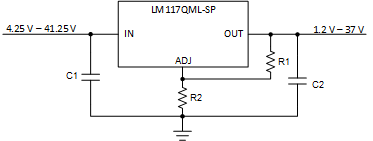
The LM117QML-SP 3-terminal positive voltage linear regulator is capable of supplying either 0.5 A or 1.5 A over a 1.2-V to 37-V output range. It is simple to use and requires only two external resistors to set the output voltage.
The regulator is "floating" and sees only the input-to-output differential voltage, thus enabling supplies of several hundred volts to be regulated as long as the maximum input-to-output differential is not exceeded.
The flight-proven LM117QML-SP offers full overload protection such as current limit, thermal overload protection, and safe area protection. It is exceptionally versatile and can also be used as an adjustable switching regulator, a programmable output regulator, a precision current regulator, and more.
 Typical Schematic
For high voltage applications, the LM117HVQML-SP is a pin-to-pin drop-in replacement suitable for up to 60 V. For the negative complement of the LM117QML-SP, see the LM137QML-SP.
| PART NUMBER(1) | GRADE(2) | PACKAGE(3) |
|---|---|---|
| LM117GWRLQMLV | LDR Flight grade QMLV RHA 100 krad(Si) |
CFP SOIC (NAC) 16 pin 6.35 mm × 9.91 mm Mass = 0.467 g(5) |
| 5962R9951707VZA | ||
| LM117GWRQMLV | HDR Flight grade QMLV RHA 100 krad(Si) |
|
| 5962R9951706VZA | ||
| LM117HRLQMLV | LDR Flight grade QMLV RHA 100 krad(Si) |
TO-39 (NDT) 3 pin 8.26 mm × 8.26 mm Mass = 1.036 g(5) |
| 5962R9951705VXA | ||
| LM117HRQMLV | HDR Flight grade QMLV RHA 100 krad(Si) |
|
| 5962R9951703VXA | ||
| LM117NDT/EM | Engineering samples(4) | |
| LM117KRQMLV | HDR Flight grade QMLV RHA 100 krad(Si) |
TO-3 (K) 2 pin 25.4 mm × 38.94 mm Mass = 12.291 g(5) |
| 5962R9951704VYA | ||
| LM117K/EM | Engineering samples(4) | |
| LM117H MDE | LDR Flight grade QMLV RHA 100 krad(Si) |
Die 2.18 mm × 2.36 mm |
| 5962R9951705V9A | ||
| LM117H MDR | HDR Flight grade QMLV RHA 100 krad(Si) |
|
| 5962R9951703V9A |