SNVS313F December 2010 – August 2018 LM137QML
PRODUCTION DATA.
- 1 Features
- 2 Applications
- 3 Description
- 4 Revision History
- 5 Pin Configuration and Functions
-
6 Specifications
- 6.1 Absolute Maximum Ratings
- 6.2 ESD Ratings
- 6.3 Recommended Operating Conditions
- 6.4 Thermal Information
- 6.5 Quality Conformance Inspection
- 6.6 LM137H 883 Electrical Characteristics DC Parameters
- 6.7 LM137H 883 Electrical Characteristics AC Parameters
- 6.8 LM137K 883 Electrical Characteristics DC Parameters
- 6.9 LM137K 883 Electrical Characteristics AC Parameters
- 6.10 LM137H RH Electrical Characteristics DC Parameters 5962P9951708VXA
- 6.11 LM137H RH Electrical Characteristics AC Parameters 5962P9951708VXA
- 6.12 LM137H RH Electrical Characteristics DC Parameters Drift Values 5962P9951708VXA
- 6.13 LM137H RH Electrical Characteristics DC Parameters Post Radiation Limits +25°C 5962P9951708VXA
- 6.14 Typical Performance Characteristics
- 7 Detailed Description
- 8 Application and Implementation
- 9 Power Supply Recommendations
- 10Device and Documentation Support
- 11Mechanical, Packaging, and Orderable Information
Package Options
Mechanical Data (Package|Pins)
- NDT|3
Thermal pad, mechanical data (Package|Pins)
Orderable Information
9.1 Thermal Regulation
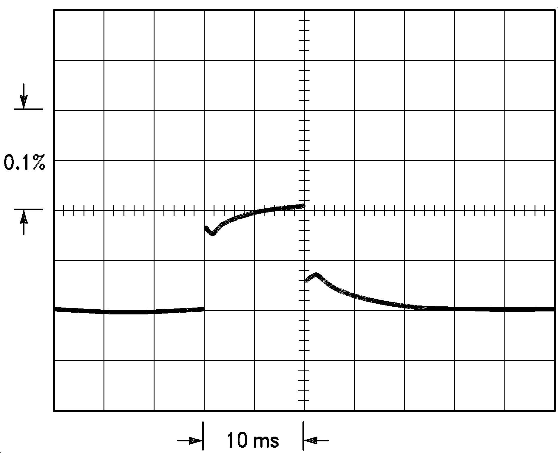
When power is dissipated in an IC, a temperature gradient occurs across the IC chip affecting the individual IC circuit components. With an IC regulator, this gradient can be especially severe since power dissipation is large. Thermal regulation is the effect of these temperature gradients on output voltage (in percentage output change) per Watt of power change in a specified time. Thermal regulation error is independent of electrical regulation or temperature coefficient, and occurs within 5 ms to 50 ms after a change in power dissipation. Thermal regulation depends on IC layout as well as electrical design. The thermal regulation of a voltage regulator is defined as the percentage change of VOUT, per Watt, within the first 10 ms after a step of power is applied. The LM137's specification is 0.02%/W, max.

| LM137, VOUT = −10V | VIN − VOUT = −40V | ||
| Horizontal sensitivity,5 ms/div | IL = 0A → 0.25A → 0A |
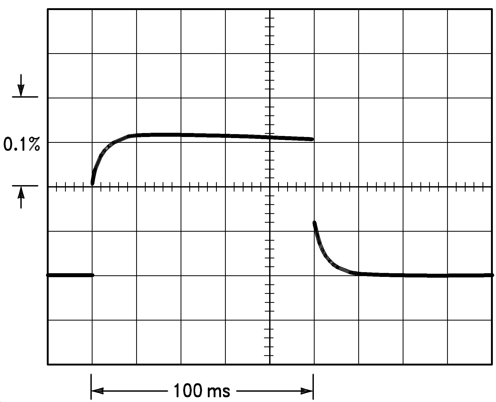
In Figure 21, a typical LM137's output drifts only 3 mV (or 0.03% of VOUT = −10V) when a 10W pulse is applied for 10 ms. This performance is thus well inside the specification limit of 0.02%/W × 10W = 0.2% max. When the 10W pulse is ended, the thermal regulation again shows a 3 mV step as the LM137 chip cools off. Note that the load regulation error of about 8 mV (0.08%) is additional to the thermal regulation error. In Figure 22, when the 10W pulse is applied for 100 ms, the output drifts only slightly beyond the drift in the first 10 ms, and the thermal error stays well within 0.1% (10 mV).

| LM137, VOUT = −10V | VIN − VOUT = −40V | ||
| Horizontal sensitivity, 20 ms/div | IL = 0A → 0.25A → 0A |