SNVS446D June   2006  – January 2016 LM1771

PRODUCTION DATA.  

  1. Features
  2. Applications
  3. Description
  4. Revision History
  5. Pin Configuration and Functions
  6. Specifications
    1. 6.1 Absolute Maximum Ratings
    2. 6.2 ESD Ratings
    3. 6.3 Recommended Operating Conditions
    4. 6.4 Thermal Information
    5. 6.5 Electrical Characteristics
    6. 6.6 Typical Characteristics
  7. Detailed Description
    1. 7.1 Overview
    2. 7.2 Functional Block Diagram
    3. 7.3 Feature Description
      1. 7.3.1 Timing Opinion
      2. 7.3.2 Short-Circuit Protection
      3. 7.3.3 Precision Enable
      4. 7.3.4 Soft-Start
      5. 7.3.5 Jitter
    4. 7.4 Device Functional Modes
  8. Application and Implementation
    1. 8.1 Application Information
    2. 8.2 Typical Applications
      1. 8.2.1 LM1771 Typical Application
        1. 8.2.1.1 Design Requirements
        2. 8.2.1.2 Detailed Design Procedure
          1. 8.2.1.2.1 Design Guide
            1. 8.2.1.2.1.1 Frequency Selection
            2. 8.2.1.2.1.2 Inductor Selection
            3. 8.2.1.2.1.3 Output Capacitor
            4. 8.2.1.2.1.4 Feedforward Capacitor
            5. 8.2.1.2.1.5 Input Capacitor
          2. 8.2.1.2.2 MOSFET Selection
            1. 8.2.1.2.2.1 VDS Voltage Rating
            2. 8.2.1.2.2.2 RDSON
            3. 8.2.1.2.2.3 Gate Drive
            4. 8.2.1.2.2.4 Gate Charge
            5. 8.2.1.2.2.5 Rise and Fall Times
            6. 8.2.1.2.2.6 Gate Charge Ratio
            7. 8.2.1.2.2.7 Feedback Resistors
          3. 8.2.1.2.3 Efficiency Calculations
            1. 8.2.1.2.3.1 Quiescent Current
            2. 8.2.1.2.3.2 Conduction Loss
            3. 8.2.1.2.3.3 Switching Loss
            4. 8.2.1.2.3.4 Transitional Loss
            5. 8.2.1.2.3.5 DCR Loss
            6. 8.2.1.2.3.6 Efficiency
        3. 8.2.1.3 Application Curve
      2. 8.2.2 Example Application 5 VIN to 1.8 VOUT
      3. 8.2.3 Example Application 5 VIN to 3.3 VOUT
  9. Power Supply Recommendations
  10. 10Layout
    1. 10.1 Layout Guidelines
    2. 10.2 Layout Examples
    3. 10.3 Thermal Considerations
  11. 11Device and Documentation Support
    1. 11.1 Device Support
      1. 11.1.1 Third-Party Products Disclaimer
    2. 11.2 Documentation Support
      1. 11.2.1 Related Documentation
    3. 11.3 Community Resources
    4. 11.4 Trademarks
    5. 11.5 Electrostatic Discharge Caution
    6. 11.6 Glossary
  12. 12Mechanical, Packaging, and Orderable Information

Package Options

Mechanical Data (Package|Pins)
Thermal pad, mechanical data (Package|Pins)
Orderable Information

1 Features

  • Input Voltage Range of 2.8 V to 5.5 V
  • 0.8-V Reference Voltage
  • Precision Enable
  • No Compensation Required
  • Constant Frequency Across Input Range
  • Low Quiescent Current of 400 µA
  • Internal Soft-Start
  • Short Circuit Protection
  • 6-Pin WSON Package and 8-Pin VSSOP Package

2 Applications

  • Simple-to-Design, High-Efficiency, Step-Down Switching Regulators
  • FPGAs, DSPs, and ASIC Power Supplies
  • Set-Top Boxes
  • Cable Modems
  • Printers
  • Digital Video Recorders
  • Servers
  • Graphic Cards

3 Description

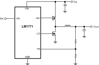
The LM1771 device is an efficient synchronous buck switching controller with a precision enable requiring no external compensation. The constant ON-time control scheme provides a simple design free of compensation components, allowing minimal component count and board space. The precision enable pin allows flexibility in sequencing multiple rails and setting UVLO. The LM1771 also incorporates a unique input feedforward to maintain a constant frequency independent of the input voltage. The LM1771 is optimized for a low-voltage input range of 2.8 V to 5.5 V and can provide an adjustable output as low as 0.8 V. Driving an external high-side PFET and low-side NFET, it can provide efficiencies as high as 95%.

Three versions of the LM1771 are available depending on the switching frequency desired for the application. Nominal switching frequencies are in the range of 100 kHz to 1000 kHz.

Device Information(1)

PART NUMBER PACKAGE BODY SIZE (NOM)
LM1771 WSON (6) 3.00 mm × 3.00 mm
VSSOP (8) 3.00 mm × 3.00 mm
  1. For all available packages, see the orderable addendum at the end of the data sheet.

Typical Application Circuit
LM1771 20189001.gif