SNVS446D June   2006  – January 2016 LM1771

PRODUCTION DATA.  

  1. Features
  2. Applications
  3. Description
  4. Revision History
  5. Pin Configuration and Functions
  6. Specifications
    1. 6.1 Absolute Maximum Ratings
    2. 6.2 ESD Ratings
    3. 6.3 Recommended Operating Conditions
    4. 6.4 Thermal Information
    5. 6.5 Electrical Characteristics
    6. 6.6 Typical Characteristics
  7. Detailed Description
    1. 7.1 Overview
    2. 7.2 Functional Block Diagram
    3. 7.3 Feature Description
      1. 7.3.1 Timing Opinion
      2. 7.3.2 Short-Circuit Protection
      3. 7.3.3 Precision Enable
      4. 7.3.4 Soft-Start
      5. 7.3.5 Jitter
    4. 7.4 Device Functional Modes
  8. Application and Implementation
    1. 8.1 Application Information
    2. 8.2 Typical Applications
      1. 8.2.1 LM1771 Typical Application
        1. 8.2.1.1 Design Requirements
        2. 8.2.1.2 Detailed Design Procedure
          1. 8.2.1.2.1 Design Guide
            1. 8.2.1.2.1.1 Frequency Selection
            2. 8.2.1.2.1.2 Inductor Selection
            3. 8.2.1.2.1.3 Output Capacitor
            4. 8.2.1.2.1.4 Feedforward Capacitor
            5. 8.2.1.2.1.5 Input Capacitor
          2. 8.2.1.2.2 MOSFET Selection
            1. 8.2.1.2.2.1 VDS Voltage Rating
            2. 8.2.1.2.2.2 RDSON
            3. 8.2.1.2.2.3 Gate Drive
            4. 8.2.1.2.2.4 Gate Charge
            5. 8.2.1.2.2.5 Rise and Fall Times
            6. 8.2.1.2.2.6 Gate Charge Ratio
            7. 8.2.1.2.2.7 Feedback Resistors
          3. 8.2.1.2.3 Efficiency Calculations
            1. 8.2.1.2.3.1 Quiescent Current
            2. 8.2.1.2.3.2 Conduction Loss
            3. 8.2.1.2.3.3 Switching Loss
            4. 8.2.1.2.3.4 Transitional Loss
            5. 8.2.1.2.3.5 DCR Loss
            6. 8.2.1.2.3.6 Efficiency
        3. 8.2.1.3 Application Curve
      2. 8.2.2 Example Application 5 VIN to 1.8 VOUT
      3. 8.2.3 Example Application 5 VIN to 3.3 VOUT
  9. Power Supply Recommendations
  10. 10Layout
    1. 10.1 Layout Guidelines
    2. 10.2 Layout Examples
    3. 10.3 Thermal Considerations
  11. 11Device and Documentation Support
    1. 11.1 Device Support
      1. 11.1.1 Third-Party Products Disclaimer
    2. 11.2 Documentation Support
      1. 11.2.1 Related Documentation
    3. 11.3 Community Resources
    4. 11.4 Trademarks
    5. 11.5 Electrostatic Discharge Caution
    6. 11.6 Glossary
  12. 12Mechanical, Packaging, and Orderable Information

Package Options

Mechanical Data (Package|Pins)
Thermal pad, mechanical data (Package|Pins)
Orderable Information

5 Pin Configuration and Functions

NGG Package
6-Pin WSON
Top View
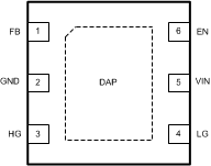
LM1771 20189002.gif
DGK Package
8-Pin VSSOP
Top View
LM1771 20189040.gif

Pin Functions

PIN TYPE(1) DESCRIPTION
NAME WSON VSSOP
DAP GND Die Attach Pad is internally connected to GND, but it cannot be used as the primary GND connection
EN 6 8 I Enable Pin
FB 1 1 A Feedback Pin
GND 2 2, 3 GND Ground
HG 3 4 AO PFET Gate Drive
LG 4 5 AO NFET Gate Drive
VIN 5 6, 7 PWR Input Supply
(1) I = Input, A = Analog, GND = Ground, AO = Analog output, PWR = Power