SNVS446D June 2006 – January 2016 LM1771
PRODUCTION DATA.
- 1 Features
- 2 Applications
- 3 Description
- 4 Revision History
- 5 Pin Configuration and Functions
- 6 Specifications
- 7 Detailed Description
-
8 Application and Implementation
- 8.1 Application Information
- 8.2 Typical Applications
- 9 Power Supply Recommendations
- 10Layout
- 11Device and Documentation Support
- 12Mechanical, Packaging, and Orderable Information
Package Options
Mechanical Data (Package|Pins)
Thermal pad, mechanical data (Package|Pins)
Orderable Information
8 Application and Implementation
NOTE
Information in the following applications sections is not part of the TI component specification, and TI does not warrant its accuracy or completeness. TI’s customers are responsible for determining suitability of components for their purposes. Customers must validate and test their design implementation to confirm system functionality.
8.1 Application Information
Design Guide details the design procedure to follow for the typical application. Because of the nature of constant ON-time controller, a certain degree of iteration might be necessary on the sizing of some key components to achieve optimal response, such as the inductor L1.
8.2 Typical Applications
8.2.1 LM1771 Typical Application
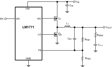 Figure 19. Example Circuit Schematic
8.2.1.1 Design Requirements
The main parameters needed to successfully design an application based on the LM1171 are typical of buck DC–DC converters. The input and output voltage must be known as well as the worst-case input voltage operating conditions. The maximum output current helps the designer size the inductor appropriately. In addition, the designer needs to be aware of the requirement on the output capacitor to achieve stable operation. See Output Capacitor for details on the output capacitor requirements.
8.2.1.2 Detailed Design Procedure
8.2.1.2.1 Design Guide
As with any DC–DC converter, numerous trade-offs are possible to optimize the design for efficiency, size, or performance. These are taken into account and highlighted throughout this discussion.
Equation 7 calculates for any buck converter is duty-cycle. Ignoring conduction losses associated with the FETs and parasitic resistances it can be approximated by:

A more accurate calculation for duty-cycle can be used that takes into account the voltage drops across the FETs. Equation 8 determines the slight load dependency on switch frequency if needed. Otherwise the simplified equation works well for component calculation.

8.2.1.2.1.1 Frequency Selection
The LM1771 is available with three preset timing options that select the ON-time and hence determine the switching frequency of the application. Increasing the switching frequency has the effect of reducing the inductor size needed for the application while requiring a slight trade-off in efficiency. Table 4 shows the same frequency table as shown earlier (Table 2) with the exception that the recommended timing option for each VOUT is highlighted. TI does not recommend using a high switching frequency with VOUT equal to or greater than 2.5 V due to the maximum duty-cycle limitations of the device coupled with the internal start-up.
Table 4. Recommended Switching Frequency vs VOUT
| VOUT | TIMING OPTIONS (1) | ||
|---|---|---|---|
| 500 ns | 1000 ns | 2000 ns | |
| 0.8 | 485 | 242 | - |
| 1 | 606 | 303 | - |
| 1.2 | 727 | 364 | - |
| 1.5 | 909 | 455 | 2237 |
| 1.8 | - | 545 | 273 |
| 2.5 | - | - | 379 |
| 3.3 | - | - | 500 |
8.2.1.2.1.2 Inductor Selection
The inductor selection is an iterative process likely requiring several passes before settling on a final value. The reason for this is because it influences the amount of ripple seen at the output, a critical component to ensure general stability of an adaptive ON-time circuit. For the first pass at inductor selection the value can be obtained by targeting a maximum peak-to-peak ripple current equal to 30% of the maximum load current. The inductor current ripple (ΔIL) can be calculated by Equation 9:

Therefore, L can be initially set by applying the 30% rule in Equation 10:

The other features of the inductor that can be selected besides inductance value are saturation current and core material. Because the LM1771 does not have a current limit, TI recommends having a saturation current higher than the maximum output current to handle any ripple or momentary overcurrent events. The core material also influences the saturation characteristics as ferrite materials have a hard saturation curve and take care that they never saturate during normal use. A shielded inductor or low-profile unshielded inductor is recommended to reduce EMI. This also helps prevent any spurious noise from picking up on the feedback node resulting in unexpected tripping of the feedback comparator.
8.2.1.2.1.3 Output Capacitor
One of the most important components to select with the LM1771 is the output capacitor. This is because its size and ESR have a direct effect on the stability of the loop. A constant ON-time control scheme works by sensing the output voltage ripple and switching the FETs appropriately. The output voltage ripple on a buck converter can be approximated by stating that the AC inductor ripple flows entirely into the output capacitor and is created by the ESR of the capacitor. This can be expressed in Equation 11:
To ensure stability, two constraints need to be met. The first is that there is sufficient ESR to create enough voltage ripple at the feedback pin. TI recommends having at least 10 mV of ripple seen at the feedback pin. This can be calculated by multiplying the output voltage ripple by the gain seen through the feedback resistors. This gain, H, can be calculated in Equation 12:

If the output voltage is fairly high, causing significant attenuation through the feedback resistors, a feedforward capacitor can be used. This is actually recommended for most circuits as it improves performance. See the Feedforward Capacitor section for more details.
The second criteria is to ensure that there is sufficient ripple at the output that is in-phase with the switch. The problem exists that there is actually ripple caused by the capacitor charging and discharging, not only the ESR ripple. Because these are effectively out of phase, problems can exist. To avoid this issue, TI recommends that the ratio of the two ripples (β) is always greater than 5. To calculate the minimum ESR value needed, Equation 13 can be used:

In general, the best capacitors to use are chemistries that have a known and consistent ESR across the entire operating temperature range. Tantalum capacitors or similar chemistries such as Niobium Oxide perform well along with certain families of Aluminum Electrolytics. Small value POSCAPs and SP CAPs also work as they have sufficient ESR. When used in conjunction with a low-value inductor it is possible to have an extremely stable design. The only capacitors that require modification to the circuit are ceramic capacitors. Ceramic capacitors cause problems meeting both criteria because they have low ESR and low capacitance. Therefore, if they are to be used, an external ESR resistor (RSNS) must be added. This can be seen in Figure 20.
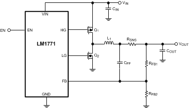 Figure 20. LM1771 With an External ESR Resistor (RSNS)
This circuit uses an additional resistor in series with the inductor to add ripple at the output. It is placed in this location and used in combination with the feedforward capacitor (CFF) to provide ripple to the feedback pin, without adding ripple or a DC offset to the output. The benefit of using a ceramic capacitor is still obtained with this technique. Because the addition of the resistor results in power loss, this circuit implementation is only recommended for low currents (2 A and below). The power loss and rating of the resistor must be taken into account when selecting this component.
This circuit implementation using the feedforward capacitor begins to experience limitations when the output voltage is small. Previously the circuit relied on the CFF for all the ripple at the feedback node by assuming that the resistor divider was negligible. As VOUT decreases this can not be assumed. The resistor divider contributes a larger amount of ripple which is problematic as it is also out of phase. Therefore the resistor location must be changed to be in series with the output capacitor. This can be viewed as adding an effective ESR to the output capacitor. This can be seen in Figure 21.
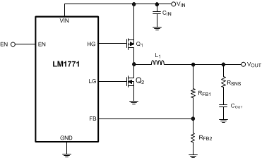 Figure 21. LM1771 With ESR Resistor (RSNS) in Series With Output Capacitor
8.2.1.2.1.4 Feedforward Capacitor
The feedforward capacitor is used across the top feedback resistor to provide a lower impedance path for the high-frequency ripple without degrading the DC accuracy. Typically the value for this capacitor must be small enough to prevent load transient errors because of the discharging time, but large enough to prevent attenuation of the ripple voltage. In general a small ceramic capacitor in the range of 1 nF to 10 nF is sufficient.
If CFF is used then it can be assumed that the ripple voltage seen at the feedback pin is the same as the ripple voltage at the output. The attenuation factor H no longer needs to be used. However, in these conditions, TI recommends having a minimum of 20-mV ripple at the feedback pin. The use of a CFF capacitor is recommended as it improves the regulation and stability of the design. However, its benefit is diminished as VOUT starts approaching VREF , therefore it is not needed in this situation.
8.2.1.2.1.5 Input Capacitor
The dominating factor that usually sets the size of an input capacitor is the current handling ability. This is usually determined by the package size and ESR of the capacitor. If these two criteria are met then there usually must be enough capacitance to prevent impedance interactions with the source. In general, TI recommends using a ceramic capacitor for the input as they provide a low impedance and small footprint.
NOTE
Use a good dielectric for the ceramic capacitor such as X5R or X7R. These provide better over temperature performance and also minimize the DC voltage derating that occurs on Y5V capacitors.
To calculate the input capacitor RMS current, Equation 14 can be used:

which can be approximated by, Equation 15

8.2.1.2.2 MOSFET Selection
The two FETs used in the LM1771 requires attention to selection of parameters to ensure optimal performance of the power supply. The high-side FET must be a PFET and the low-side an NFET. These can be integrated in one package or as two separate packages.
8.2.1.2.2.1 VDS Voltage Rating
The first selection criteria is to select FETs that have sufficient VDS voltage ratings to handle the maximum voltage seen at the input plus any transient spikes that can occur from parasitic ringing. In general most FETs available for this application have ratings from 8 V to 20 V. If a larger voltage rating is used then the performance is most likely be degraded because of higher gate capacitance.
8.2.1.2.2.2 RDSON
The RDS(ON) specification is important as it determines several attributes of the FET and the overall power supply. The first is that it sets the maximum current of the FET for a given package. A lower RDS(ON) permits a higher allowable current and reduce conduction losses, however, it increases the gate capacitance and the switching losses.
8.2.1.2.2.3 Gate Drive
The next step is to ensure that the FETs are capable of switching at the low Vin supplies used by the LM1771. The FET must have the Rdson specified at either 1.8 V or 2.5 V to ensure that it can switch effectively as soon as the LM1771 starts up.
8.2.1.2.2.4 Gate Charge
Because the LM1771 uses a fixed dead-time scheme to prevent cross conduction, the FET transitions must occur in this time. The rise and fall time of the FETs gate can be influenced by several factors including the gate capacitance. Therefore the total gate charge of both FETs must be limited to less than 20 nC at 4.5 V VGS. The lower the number the faster the FETs must switch and the better the efficiency.
8.2.1.2.2.5 Rise and Fall Times
A better indication of the actual switching times of the FETs can be found in their Electrical Characteristics table. The rise and fall time must be specified and selected to be at a minimum. This helps improve efficiency and ensuring that shoot-through does not occur.
8.2.1.2.2.6 Gate Charge Ratio
Another consideration in selecting the FETs is to pay attention to the Qgd / Qgs ratio. The reason for this is that proper selection can prevent spurious turnon. If we look at the NFET for example, when the FET is turning off, the gate signal pulls to ground. Conversely the PFET is turning on, causing the SW node to rise towards VIN. The gate-to-drain capacitance of the NFET couples the SW node to the gate and causes it to rise. If this voltage is excessive, then it could weakly turn on the low-side FET causing an efficiency loss. However, this coupling is mitigated by having a large gate to source capacitance of the FET, which helps to hold the gate voltage down. Ideally, a very low Qgd / Qgs would be ideal, but in practice it is common to find the number around 1. As a general rule, the lower the ratio, the better.
If the above selection criteria have been met it is useful to generate a figure of merit to allow comparison between the FETs. One such method is to multiply the RDS(ON) of the FET by the total gate charge. This allows an easy comparison of the different FETs available. Once again, the lower the product, the better.
8.2.1.2.2.7 Feedback Resistors
The feedback resistors are used to scale the output voltage to the internal reference value such that the loop can be regulated. The feedback resistors must not be made arbitrarily large as this creates a high impedance node at the feedback pin that is more susceptible to noise. A combined value of 50 kΩ for the two resistors is adequate. To calculate the resistor values use Equation 16. Typically, the low-side resistor is initially set to a predetermined value such as 10 kΩ.

where
- VFB is the internal reference voltage that can be found in the Electrical Characteristics table or approximated by 0.8 V
The output voltage value can be set in a precise manner by taking into account the fact that the reference voltage is regulating the bottom of the output ripple as opposed to the average value. This relationship is shown in Figure 22.
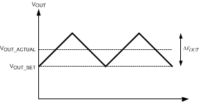 Figure 22. Output Voltage Waveform
The average output voltage (VOUT_ACTUAL) is higher than the output voltage (VOUT_SET) that was calculated by the earlier equation by exactly half the output voltage ripple. The output voltage that is targeted for regulation may then be appended according to the voltage ripple. This can be seen in Equation 17:
8.2.1.2.3 Efficiency Calculations
One of the most important parameters to calculate during the design stage is the expected efficiency of the system. This can help determine optimal FET selection and can be used to calculate expected temperature rise of the individual components.
8.2.1.2.3.1 Quiescent Current
The quiescent current consumed by the LM1771 is one of the major sources of loss within the controller. However, from a system standpoint this is usually less than 0.5% of the overall efficiency. Therefore, it could easily be omitted but is shown for completeness:
8.2.1.2.3.2 Conduction Loss
There are three losses associated with the external FETs. From the DC standpoint there is the I-squared R loss, caused by the ON-resistance of the FET. This can be modeled for the PMOS by:
and the NMOS by:
8.2.1.2.3.3 Switching Loss
The next loss is the switching loss that is caused by the need to charge and discharge the gate capacitance of the FETs every cycle. This can be approximated by:
for the PMOS, and the same approach can be adapted for the NMOS:
8.2.1.2.3.4 Transitional Loss
The last FET power loss is the transitional loss. This is caused by switching the PMOS while it is conducting current. This approach only models the PMOS transition, the NMOS loss is considered negligible because it has minimal drain to source voltage when it switches due to the conduction of the body diode. Therefore the transitional loss of the PMOS can be modeled by:
tr and tf are the rise and fall times of the FET and can be found in their corresponding datasheet. Typically these numbers are simulated using a 6-Ω drive, which corresponds well to the LM1771. Given this, no adjustment is needed.
8.2.1.2.3.5 DCR Loss
The last source of power loss in the system that needs to be calculated is the loss associated with the inductor resistance (DCR) which can be calculated by Equation 24:
8.2.1.2.3.6 Efficiency
The efficiency, η, can then be calculated by summing all the power losses and then using Equation 25:

8.2.1.3 Application Curve
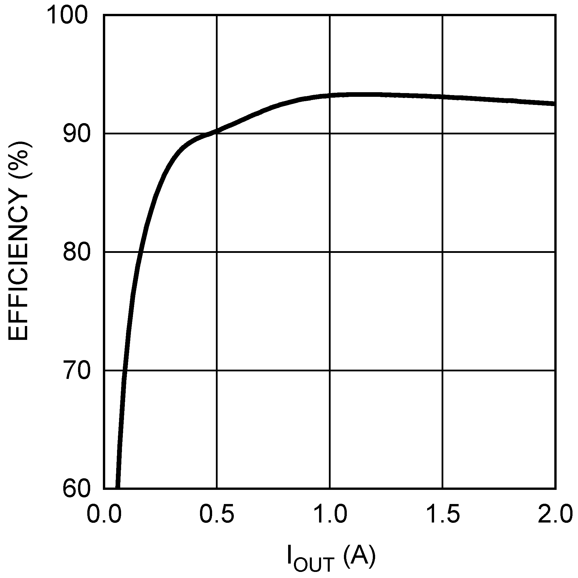 Figure 23. Typical Efficiency 5 VIN to 2.5 VOUT
8.2.2 Example Application 5 VIN to 1.8 VOUT
Figure 24 and Table 5 show an application with conversion from 5-V input to 1.8-V output with a switching frequency of 1.1 MHz and a 2-A maximum output current.
 Figure 24. Example Circuit Schematic, 5 VIN to 1.8 VOUT
Table 5. Bill of Materials (5-V to 1.8-V Conversion, fSW = 1090 kHz, IOUT = 2 A)
| DESIGNATOR | DESCRIPTION | PART NUMBER | QUANTITY | VENDOR |
|---|---|---|---|---|
| U1 | LM1771, 500 ns | LM1771S | 1 | Texas Instruments |
| Q1 | PMOS | Si3867DV | 1 | Siliconix |
| Q2 | NMOS | Si3460DV | 1 | Siliconix |
| CIN | 22-μF Capacitor, 0805 | GRM21BR60J226ME39 | 1 | Murata |
| COUT | 100-μF Capacitor, 6.3 V, 100 mΩ | TPSY107M006R0100 | 1 | AVX |
| RFB1 | 12.4-kΩ Resistor, 0603 | CRCW06031242F | 1 | Vishay |
| RFB2 | 10-kΩ Resistor, 0603 | CRCW06031002F | 1 | Vishay |
| CFF | 1-nF Capacitor, 0603 | VJ0603102KXXA | 1 | Vishay |
| L | 3.3-μH Inductor | MSS7341-332NLB | 1 | Coilcraft |
8.2.3 Example Application 5 VIN to 3.3 VOUT
Figure 25 and Table 6 show an application with conversion from 5-V input to 3.3-V output with a switching frequency of 500 kHz and a 5-A maximum output current.
 Figure 25. Example Circuit Schematic, 5 VIN to 3.3 VOUT
Table 6. Bill of Materials (5-V to 3.3-V Conversion, fSW = 500 kHz, IOUT = 5 A)
| DESIGNATOR | DESCRIPTION | PART NUMBER | QUANTITY | VENDOR |
|---|---|---|---|---|
| U1 | LM1771, 200 ns | LM1771U | 1 | Texas Instruments |
| Q1 | PMOS | Si9433BDY | 1 | Siliconix |
| Q2 | NMOS | Si4894DY | 1 | Siliconix |
| CIN | 100-μF Capacitor, 1812 | GRM43SR60J107ME20B | 1 | Murata |
| COUT | 150-μF Capacitor, 6.3 V, 70 mΩ | NOSD157M006R0070 | 1 | AVX |
| RFB1 | 29.4-kΩ Resistor, 0805 | CRCW08052942F | 1 | Vishay |
| RFB2 | 10-kΩ Resistor, 0805 | CRCW08051002F | 1 | Vishay |
| CFF | 1-nF Capacitor, 0805 | VJ0805102KXXA | 1 | Vishay |
| L | 2.2-μH Inductor | DO3316P-222 | 1 | Coilcraft |