SNVS715B March   2011  – June 2019 LM21212-2

PRODUCTION DATA.  

  1. Features
  2. Applications
  3. Description
    1.     Device Images
      1.      Simplified Application Circuit
  4. Revision History
  5. Description, continued
  6. Pin Configuration and Functions
    1.     Pin Descriptions
  7. Specifications
    1. 7.1 Absolute Maximum Ratings
    2. 7.2 ESD Ratings
    3. 7.3 Recommended Operating Ratings
    4. 7.4 Electrical Characteristics
    5. 7.5 Typical Characteristics
  8. Detailed Description
    1. 8.1 Overview
    2. 8.2 Functional Block Diagram
    3. 8.3 Feature Description
      1. 8.3.1 Precision Enable
      2. 8.3.2 UVLO
      3. 8.3.3 Current Limit
      4. 8.3.4 Short-Circuit Protection
      5. 8.3.5 Thermal Protection
      6. 8.3.6 Power-Good Flag
      7. 8.3.7 Light Load Operation
    4. 8.4 Device Functional Modes
  9. Application and Implementation
    1. 9.1 Application Information
    2. 9.2 Typical Application
      1. 9.2.1 Typical Application 1
        1. 9.2.1.1 Design Requirements
        2. 9.2.1.2 Detailed Design Procedure
          1. 9.2.1.2.1 Custom Design With WEBENCH® Tools
          2. 9.2.1.2.2 Output Voltage
          3. 9.2.1.2.3 Precision Enable
          4. 9.2.1.2.4 Soft Start
          5. 9.2.1.2.5 Resistor-Adjustable Frequency
          6. 9.2.1.2.6 Inductor Selection
          7. 9.2.1.2.7 Output Capacitor Selection
          8. 9.2.1.2.8 Input Capacitor Selection
          9. 9.2.1.2.9 Control Loop Compensation
        3. 9.2.1.3 Application Curves
      2. 9.2.2 Typical Application Schematic 2
        1. 9.2.2.1 Design Requirements
        2. 9.2.2.2 Detailed Design Procedure
  10. 10Layout
    1. 10.1 Layout Considerations
    2. 10.2 Layout Example
    3. 10.3 Thermal Considerations
  11. 11Device and Documentation Support
    1. 11.1 Device Support
      1. 11.1.1 Third-Party Products Disclaimer
      2. 11.1.2 Development Support
        1. 11.1.2.1 Custom Design With WEBENCH® Tools
    2. 11.2 Receiving Notification of Documentation Updates
    3. 11.3 Community Resources
    4. 11.4 Trademarks
    5. 11.5 Electrostatic Discharge Caution
    6. 11.6 Glossary
  12. 12Mechanical, Packaging, and Orderable Information

Package Options

Mechanical Data (Package|Pins)
Thermal pad, mechanical data (Package|Pins)
Orderable Information

Power-Good Flag

The PGOOD pin provides the user with a way to monitor the status of the LM21212-2. In order to use the PGOOD pin, the application must provide a pullup resistor to a desired DC voltage (in other words, VIN). PGOOD responds to a fault condition by pulling the PGOOD pin low with the open-drain output. PGOOD will pull low on the following conditions – 1) VFB moves above or below the VOVP or VUVP, respectively 2) The enable pin is brought below the enable threshold 3) The device enters a prebiased output condition (VFB>VSS).

Figure 19 shows the conditions that will cause PGOOD to fall.
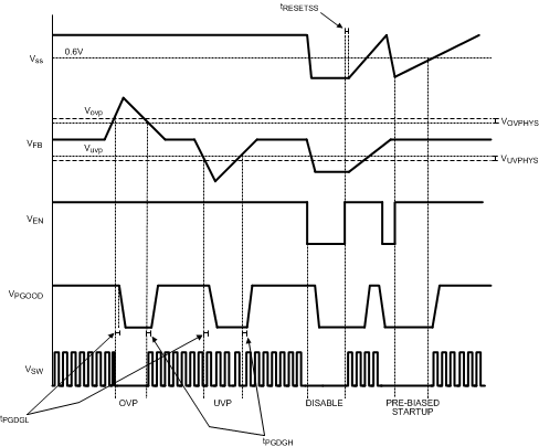
LM21212-2 30155118.gifFigure 19. PGOOD Conditions