SNVS680I August 2010 – April 2018 LM25119
PRODUCTION DATA.
- 1 Features
- 2 Applications
- 3 Description
- 4 Revision History
- 5 Pin Configuration and Functions
- 6 Specifications
-
7 Detailed Description
- 7.1 Overview
- 7.2 Functional Block Diagram
- 7.3
Feature Description
- 7.3.1 High Voltage Start-Up Regulator
- 7.3.2 UVLO
- 7.3.3 Enable 2
- 7.3.4 Oscillator and Sync Capability
- 7.3.5 Error Amplifiers and PWM Comparators
- 7.3.6 Ramp Generator
- 7.3.7 Current Limit
- 7.3.8 Hiccup Mode Current Limiting
- 7.3.9 Soft Start
- 7.3.10 HO and LO Output Drivers
- 7.3.11 Maximum Duty Cycle
- 7.3.12 Thermal Protection
- 7.4 Device Functional Modes
-
8 Application and Implementation
- 8.1 Application Information
- 8.2
Typical Applications
- 8.2.1
Dual-output Design Example
- 8.2.1.1 Design Requirements
- 8.2.1.2
Detailed Design Procedure
- 8.2.1.2.1 Timing Resistor
- 8.2.1.2.2 Output Inductor
- 8.2.1.2.3 Current Sense Resistor
- 8.2.1.2.4 Ramp Resistor and Ramp Capacitor
- 8.2.1.2.5 Output Capacitors
- 8.2.1.2.6 Input Capacitors
- 8.2.1.2.7 VCC Capacitor
- 8.2.1.2.8 Bootstrap Capacitor
- 8.2.1.2.9 Soft Start Capacitor
- 8.2.1.2.10 Restart Capacitor
- 8.2.1.2.11 Output Voltage Divider
- 8.2.1.2.12 UVLO Divider
- 8.2.1.2.13 MOSFET Selection
- 8.2.1.2.14 MOSFET Snubber
- 8.2.1.2.15 Error Amplifier Compensation
- 8.2.1.3 Application Curves
- 8.2.2 Two-Phase Design Example
- 8.2.1
Dual-output Design Example
- 9 Power Supply Recommendations
- 10Layout
- 11Device and Documentation Support
- 12Mechanical, Packaging, and Orderable Information
Package Options
Mechanical Data (Package|Pins)
- RTV|32
Thermal pad, mechanical data (Package|Pins)
- RTV|32
Orderable Information
8.2.1.2.15 Error Amplifier Compensation
RCOMP, CCOMP, and CHF configure the error amplifier gain characteristics to accomplish a stable voltage loop gain. One advantage of current mode control is the ability to close the loop with only two feedback components, RCOMP and CCOMP. The voltage loop gain is the product of the modulator gain and the error amplifier gain. For the 3.3-V output design example, the modulator is treated as an ideal voltage-to-current converter. The DC modulator gain of the LM25119 can be modeled with Equation 40.

where
- A is the gain of the current sense amplifier which is 10 in the LM25119
The dominant low frequency pole of the modulator is determined by the load resistance (RLOAD) and output capacitance (COUT). The corner frequency of this pole calculated with Equation 41.

For RLOAD = 3.3 V / 8 A = 0.413 Ω and COUT = 724 μF (effective) then fP(MOD) = 532 Hz
DC Gain(MOD) = 0.413 Ω / (10 x 8 mΩ) = 5.16 = 14.2 dB
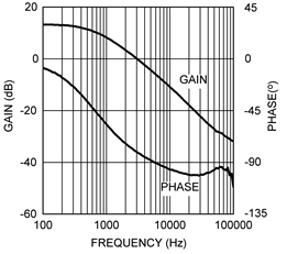
For the 3.3-V design example, the modulator gain versus frequency characteristic is shown in Figure 18.
 Figure 18. Modulator Gain and Phase
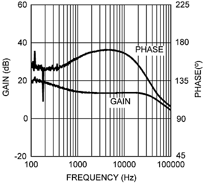
Components RCOMP and CCOMP configure the error amplifier as a Type II configuration. The DC gain of the amplifier is 80 dB with a pole at 0 Hz and a zero at fZEA = 1 / (2 π x RCOMP x CCOMP). The error amplifier zero cancels the modulator pole leaving a single pole response at the crossover frequency of the voltage loop. A single pole response at the crossover frequency yields a very stable loop with 90 degrees of phase margin. For the design example, a conservative target loop bandwidth (crossover frequency) of 11 kHz was selected. The compensation network zero (fZEA) must be selected at least an order of magnitude less than the target crossover frequency. This constrains the product of RCOMP and CCOMP for a desired compensation network zero 1 / (2 π x RCOMP x CCOMP) to be about 1.1 kHz. Increasing RCOMP, while proportionally decreasing CCOMP, increases the error amp gain. Conversely, decreasing RCOMP while proportionally increasing CCOMP, decreases the error amp gain. For the design example, CCOMP was selected as 6800 pF and RCOMP was selected as 36.5 kΩ. These values configure the compensation network zero at 640 Hz. The error amp gain at frequencies greater than fZEA is: RCOMP / RFB2, which is approximately 5.22 (14.3 dB).
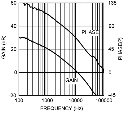
The overall voltage loop gain can be predicted as the sum (in dB) of the modulator gain and the error amp gain.
 Figure 19. Error Amplifier Gain and Phase
 Figure 20. Overall Voltage Loop Gain and Phase
If a network analyzer is available, the modulator gain can be measured and the error amplifier gain can be configured for the desired loop transfer function. If the K factor is between 2 and 3, the stability must be checked with the network analyzer. If a network analyzer is not available, the error amplifier compensation components can be designed with the guidelines given. Step load transient tests can be performed to verify acceptable performance. The step load goal is minimum overshoot with a damped response. CHF can be added to the compensation network to decrease noise susceptibility of the error amplifier. The value of CHF must be sufficiently small because the addition of this capacitor adds a pole in the error amplifier transfer function. This pole must be well beyond the loop crossover frequency.
Equation 42 offers a good approximation of the location of the pole added by CHF.
The value of CHF was selected as 100 pF for the design example.