SNVS680I August 2010 – April 2018 LM25119
PRODUCTION DATA.
- 1 Features
- 2 Applications
- 3 Description
- 4 Revision History
- 5 Pin Configuration and Functions
- 6 Specifications
-
7 Detailed Description
- 7.1 Overview
- 7.2 Functional Block Diagram
- 7.3
Feature Description
- 7.3.1 High Voltage Start-Up Regulator
- 7.3.2 UVLO
- 7.3.3 Enable 2
- 7.3.4 Oscillator and Sync Capability
- 7.3.5 Error Amplifiers and PWM Comparators
- 7.3.6 Ramp Generator
- 7.3.7 Current Limit
- 7.3.8 Hiccup Mode Current Limiting
- 7.3.9 Soft Start
- 7.3.10 HO and LO Output Drivers
- 7.3.11 Maximum Duty Cycle
- 7.3.12 Thermal Protection
- 7.4 Device Functional Modes
-
8 Application and Implementation
- 8.1 Application Information
- 8.2
Typical Applications
- 8.2.1
Dual-output Design Example
- 8.2.1.1 Design Requirements
- 8.2.1.2
Detailed Design Procedure
- 8.2.1.2.1 Timing Resistor
- 8.2.1.2.2 Output Inductor
- 8.2.1.2.3 Current Sense Resistor
- 8.2.1.2.4 Ramp Resistor and Ramp Capacitor
- 8.2.1.2.5 Output Capacitors
- 8.2.1.2.6 Input Capacitors
- 8.2.1.2.7 VCC Capacitor
- 8.2.1.2.8 Bootstrap Capacitor
- 8.2.1.2.9 Soft Start Capacitor
- 8.2.1.2.10 Restart Capacitor
- 8.2.1.2.11 Output Voltage Divider
- 8.2.1.2.12 UVLO Divider
- 8.2.1.2.13 MOSFET Selection
- 8.2.1.2.14 MOSFET Snubber
- 8.2.1.2.15 Error Amplifier Compensation
- 8.2.1.3 Application Curves
- 8.2.2 Two-Phase Design Example
- 8.2.1
Dual-output Design Example
- 9 Power Supply Recommendations
- 10Layout
- 11Device and Documentation Support
- 12Mechanical, Packaging, and Orderable Information
Package Options
Mechanical Data (Package|Pins)
- RTV|32
Thermal pad, mechanical data (Package|Pins)
- RTV|32
Orderable Information
7.3.6 Ramp Generator
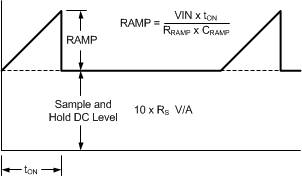
The ramp signal used in the pulse width modulator for current mode control is typically derived directly from the buck switch current. This switch current corresponds to the positive slope portion of the inductor current. Using this signal for the PWM ramp simplifies the control loop transfer function to a single pole response and provides inherent input voltage feedforward compensation. The disadvantage of using the buck switch current signal for PWM control is the large leading edge spike due to circuit parasitics that must be filtered or blanked. Also, the current measurement may introduce significant propagation delays. The filtering, blanking time, and propagation delay limit the minimum achievable pulse width. In applications where the input voltage may be relatively large in comparison to the output voltage, controlling small pulse widths and duty cycles are necessary for regulation. The LM25119 uses a unique ramp generator which does not actually measure the buck switch current but rather reconstructs the signal. Representing or emulating the inductor current provides a ramp signal to the PWM comparator that is free of leading edge spikes and measurement or filtering delays. The current reconstruction is comprised of two elements; a sample-and-hold DC level and the emulated inductor current ramp as shown in Figure 9.
 Figure 9. Composition of Current Sense Signal
The sample-and-hold DC level is derived from a measurement of the recirculating current flowing through the current sense resistor. The voltage across the sense resistor is sampled and held just prior to the onset of the next conduction interval of the buck switch. The current sensing and sample-and-hold provide the DC level of the reconstructed current signal. The positive slope inductor current ramp is emulated by an external capacitor connected from RAMP pin to AGND and a series resistor connected between SW and RAMP. The ramp resistor must not be connected to VIN directly because the RAMP pin voltage rating could be exceeded under high VIN conditions. The ramp created by the external resistor and capacitor has a slope proportional to the rising inductor current plus some additional slope required for slope compensation. Connecting the RAMP pin resistor to SW provides optimum slope compensation with a RAMP capacitor slope that is proportional to VIN. This adaptive slope compensation eliminates the requirement for additional slope compensation circuitry with high output voltage set points and frees the user from additional concerns in this area. The emulated ramp signal is approximately linear and the ramp slope is given in Equation 2.

The factor of 10 Equation 2 corresponds to the internal current sense amplifier gain of the LM25119. The K factor is a constant which adds additional slope for robust pulse-width modulation control at lower input voltages. In practice this constant can be varied from 1 to 3. RS is the external sense resistor value.
The voltage on the ramp capacitor is given with Equation 3and Equation 4.


The approximation is the first order term in a Taylor Series expansion of the exponential and is valid because tPERIOD is small relative to the RAMP pin R-C time constant.
Multiplying Equation 2 by tPERIOD to convert the slope to a peak voltage, and then equating Equation 2 with Equation 4 allows us to solve for CRAMP using Equation 5.

Choose either CRAMP or RRAMP and use Equation 5 to calculate the other component.
The difference between the average inductor current and the DC value of the sampled inductor current can cause instability for certain operating conditions. This instability is known as sub-harmonic oscillation, which occurs when the inductor ripple current does not return to its initial value by the start of next switching cycle. Sub-harmonic oscillation is normally characterized by alternating wide and narrow pulses at the switch node. The ramp equation above contains the optimum amount of slope compensation, however extra slope compensation is easily added by selecting a lower value for RRAMP or CRAMP.