SNVSAU1 March 2017 LM25141
PRODUCTION DATA.
- 1 Features
- 2 Applications
- 3 Description
- 4 Revision History
- 5 Pin Configuration and Functions
- 6 Specifications
-
7 Detailed Description
- 7.1 Overview
- 7.2 Functional Block Diagram
- 7.3
Feature Description
- 7.3.1 High Voltage Start-up Regulator
- 7.3.2 VCC Regulator
- 7.3.3 Oscillator
- 7.3.4 Synchronization
- 7.3.5 Frequency Dithering (Spread Spectrum)
- 7.3.6 Enable
- 7.3.7 Power Good
- 7.3.8 Output Voltage
- 7.3.9 Current Sense
- 7.3.10 DCR Current Sensing
- 7.3.11 Error Amplifier and PWM Comparator
- 7.3.12 Slope Compensation
- 7.3.13 Hiccup Mode Current Limiting
- 7.3.14 Standby Mode
- 7.3.15 Soft-Start
- 7.3.16 Diode Emulation
- 7.3.17 High and Low Side Drivers
- 8 Application and Implementation
- 9 Power Supply Recommendations
- 10Layout
- 11Device and Documentation Support
- 12Mechanical, Packaging, and Orderable Information
Package Options
Mechanical Data (Package|Pins)
- RGE|24
Thermal pad, mechanical data (Package|Pins)
- RGE|24
Orderable Information
8.2.6.3 Driver Slew Rate Control
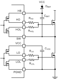
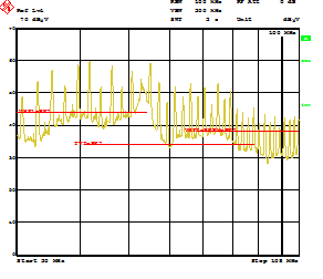
Figure 30 shows the high current driver outputs with independent source and current sink pins for slew rate control. Slew rate control enables the user to adjust the switch node rise and fall times which can reduce the conducted EMI in the FM radio band (30 MHz to 108 MHz). Figure 31 shows the measured results without slew rate control.
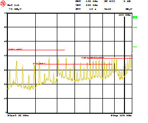
The conducted EMI results with slew rate control are shown in Figure 32, a 10-dB reduction in conduction emissions in the FM band is attained by using slew rate control. This can help reduce the size and cost of the EMI filters.
 Figure 30. Drivers with Slew Rate Control
 Figure 31. Conducted EMI Measurement, Without Slew Rate Control
 Figure 32. Conducted EMI Measurements, With Slew Rate Control