SNVSBV6B December 2020 – January 2023 LM25149-Q1
PRODUCTION DATA
- 1 Features
- 2 Applications
- 3 Description
- 4 Revision History
- 5 Description (continued)
- 6 Pin Configuration and Functions
- 7 Specifications
-
8 Detailed Description
- 8.1 Overview
- 8.2 Functional Block Diagram
- 8.3
Feature Description
- 8.3.1 Input Voltage Range (VIN)
- 8.3.2 High-Voltage Bias Supply Regulator (VCC, VCCX, VDDA)
- 8.3.3 Precision Enable (EN)
- 8.3.4 Power-Good Monitor (PG)
- 8.3.5 Switching Frequency (RT)
- 8.3.6 Active EMI Filter
- 8.3.7 Dual Random Spread Spectrum (DRSS)
- 8.3.8 Soft Start
- 8.3.9 Output Voltage Setpoint (FB)
- 8.3.10 Minimum Controllable On Time
- 8.3.11 Error Amplifier and PWM Comparator (FB, EXTCOMP)
- 8.3.12 Slope Compensation
- 8.3.13 Inductor Current Sense (ISNS+, VOUT)
- 8.3.14 Hiccup Mode Current Limiting
- 8.3.15 High-Side and Low-Side Gate Drivers (HO, LO)
- 8.3.16 Output Configurations (CNFG)
- 8.3.17 Single-Output Dual-Phase Operation
- 8.4 Device Functional Modes
-
9 Application and Implementation
- 9.1 Application Information
- 9.2
Typical Applications
- 9.2.1
Design 1 – High-Efficiency 2.1-MHz Synchronous
Buck Regulator
- 9.2.1.1 Design Requirements
- 9.2.1.2
Detailed Design Procedure
- 9.2.1.2.1 Custom Design With WEBENCH® Tools
- 9.2.1.2.2 Custom Design With Excel Quickstart Tool
- 9.2.1.2.3 Buck Inductor
- 9.2.1.2.4 Current-Sense Resistance
- 9.2.1.2.5 Output Capacitors
- 9.2.1.2.6 Input Capacitors
- 9.2.1.2.7 Frequency Set Resistor
- 9.2.1.2.8 Feedback Resistors
- 9.2.1.2.9 Compensation Components
- 9.2.1.2.10 Active EMI Components
- 9.2.1.3 Application Curves
- 9.2.2 Design 2 – High Efficiency 440-kHz Synchronous Buck Regulator
- 9.2.3 Design 3 – Dual-Phase 400-kHz 20-A Synchronous Buck Regulator
- 9.2.1
Design 1 – High-Efficiency 2.1-MHz Synchronous
Buck Regulator
- 9.3 Power Supply Recommendations
- 9.4 Layout
- 10Device and Documentation Support
- 11Mechanical, Packaging, and Orderable Information
Package Options
Mechanical Data (Package|Pins)
- RGY|24
Thermal pad, mechanical data (Package|Pins)
- RGY|24
Orderable Information
9.1.1.3 Input Capacitors
Input capacitors are necessary to limit the input ripple voltage to the buck power stage due to switching-frequency AC currents. TI recommends using X7S or X7R dielectric ceramic capacitors to provide low impedance and high RMS current rating over a wide temperature range. To minimize the parasitic inductance in the switching loop, position the input capacitors as close as possible to the drain of the high-side MOSFET and the source of the low-side MOSFET. The input capacitor RMS current for a single-channel buck regulator is given by Equation 17.
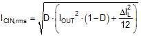
The highest input capacitor RMS current occurs at D = 0.5, at which point the RMS current rating of the input capacitors must be greater than half the output current.
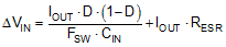
Ideally, the DC component of input current is provided by the input voltage source and the AC component by the input filter capacitors. Neglecting inductor ripple current, the input capacitors source current of amplitude (IOUT − IIN) during the D interval and sinks IIN during the 1−D interval. Thus, the input capacitors conduct a square-wave current of peak-to-peak amplitude equal to the output current. It follows that the resultant capacitive component of AC ripple voltage is a triangular waveform. Together with the ESR-related ripple component, the peak-to-peak ripple voltage amplitude is given by Equation 18.
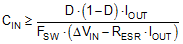
The input capacitance required for a particular load current, based on an input voltage ripple specification of ΔVIN, is given by Equation 19.
Low-ESR ceramic capacitors can be placed in parallel with higher valued bulk capacitance to provide optimized input filtering for the regulator and damping to mitigate the effects of input parasitic inductance resonating with high-Q ceramics. One bulk capacitor of sufficiently high current rating and four 10-μF 50-V X7R ceramic decoupling capacitors are usually sufficient for 12-V battery automotive applications. Select the input bulk capacitor based on its ripple current rating and operating temperature range.
Of course, a two-channel buck regulator with 180° out-of-phase interleaved switching provides input ripple current cancellation and reduced input capacitor current stress. The above equations represent valid calculations when one output is disabled and the other output is fully loaded.