SNVSBV6B December 2020 – January 2023 LM25149-Q1
PRODUCTION DATA
- 1 Features
- 2 Applications
- 3 Description
- 4 Revision History
- 5 Description (continued)
- 6 Pin Configuration and Functions
- 7 Specifications
-
8 Detailed Description
- 8.1 Overview
- 8.2 Functional Block Diagram
- 8.3
Feature Description
- 8.3.1 Input Voltage Range (VIN)
- 8.3.2 High-Voltage Bias Supply Regulator (VCC, VCCX, VDDA)
- 8.3.3 Precision Enable (EN)
- 8.3.4 Power-Good Monitor (PG)
- 8.3.5 Switching Frequency (RT)
- 8.3.6 Active EMI Filter
- 8.3.7 Dual Random Spread Spectrum (DRSS)
- 8.3.8 Soft Start
- 8.3.9 Output Voltage Setpoint (FB)
- 8.3.10 Minimum Controllable On Time
- 8.3.11 Error Amplifier and PWM Comparator (FB, EXTCOMP)
- 8.3.12 Slope Compensation
- 8.3.13 Inductor Current Sense (ISNS+, VOUT)
- 8.3.14 Hiccup Mode Current Limiting
- 8.3.15 High-Side and Low-Side Gate Drivers (HO, LO)
- 8.3.16 Output Configurations (CNFG)
- 8.3.17 Single-Output Dual-Phase Operation
- 8.4 Device Functional Modes
-
9 Application and Implementation
- 9.1 Application Information
- 9.2
Typical Applications
- 9.2.1
Design 1 – High-Efficiency 2.1-MHz Synchronous
Buck Regulator
- 9.2.1.1 Design Requirements
- 9.2.1.2
Detailed Design Procedure
- 9.2.1.2.1 Custom Design With WEBENCH® Tools
- 9.2.1.2.2 Custom Design With Excel Quickstart Tool
- 9.2.1.2.3 Buck Inductor
- 9.2.1.2.4 Current-Sense Resistance
- 9.2.1.2.5 Output Capacitors
- 9.2.1.2.6 Input Capacitors
- 9.2.1.2.7 Frequency Set Resistor
- 9.2.1.2.8 Feedback Resistors
- 9.2.1.2.9 Compensation Components
- 9.2.1.2.10 Active EMI Components
- 9.2.1.3 Application Curves
- 9.2.2 Design 2 – High Efficiency 440-kHz Synchronous Buck Regulator
- 9.2.3 Design 3 – Dual-Phase 400-kHz 20-A Synchronous Buck Regulator
- 9.2.1
Design 1 – High-Efficiency 2.1-MHz Synchronous
Buck Regulator
- 9.3 Power Supply Recommendations
- 9.4 Layout
- 10Device and Documentation Support
- 11Mechanical, Packaging, and Orderable Information
Package Options
Mechanical Data (Package|Pins)
- RGY|24
Thermal pad, mechanical data (Package|Pins)
- RGY|24
Orderable Information
8.3.15 High-Side and Low-Side Gate Drivers (HO, LO)
The LM25149-Q1 contains gate drivers and an associated high-side level shifter to drive the external N-channel power MOSFETs. The high-side gate driver works in conjunction with an internal bootstrap diode, DBOOT, and bootstrap capacitor, CBOOT. During the conduction interval of the low-side MOSFET, the SW voltage is approximately 0 V and CBOOT charges from VCC through the internal DBOOT. TI recommends a 0.1-μF ceramic capacitor connected with short traces between the CBOOT and SW pins.
The LO and HO outputs are controlled with an adaptive dead-time methodology so that both outputs (HO and LO) are never on at the same time, preventing cross conduction. Before the LO driver output is allowed to turn on, the adaptive dead-time logic first disables HO and waits for the HO voltage to drop below 2 V typical. LO is allow to turn on after a small delay (HO fall to LO rising delay). Similarly, the HO turn-on is delayed until the LO voltage has dropped below 2 V. This technique ensures adequate dead-time for any size N-channel power MOSFET implementations, including parallel MOSFET configurations.
Caution is advised when adding series gate resistors, as this can impact the effective dead-time. The selected high-side MOSFET determines the appropriate bootstrap capacitance value CBOOT in accordance with Equation 12.
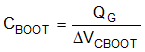
where
- QG is the total gate charge of the high-side MOSFET at the applicable gate drive voltage.
- ΔVCBOOT is the voltage variation of the high-side MOSFET driver after turn-on.
To determine CBOOT, choose ΔVCBOOT so that the available gate drive voltage is not significantly impacted. An acceptable range of ΔVCBOOT is 100 mV to 300 mV. The bootstrap capacitor must be a low-ESR ceramic capacitor, typically 0.1 µF. Use high-side and low-side MOSFETs with logic-level gate threshold voltages.