SNVS576F August 2008 – February 2015 LM26003 , LM26003-Q1
PRODUCTION DATA.
- 1 Features
- 2 Applications
- 3 Description
- 4 Typical Application Circuit
- 5 Revision History
- 6 Pin Configuration and Functions
- 7 Specifications
- 8 Detailed Description
- 9 Application and Implementation
- 10Power Supply Recommendations
- 11Layout
- 12Device and Documentation Support
- 13Mechanical, Packaging, and Orderable Information
Package Options
Mechanical Data (Package|Pins)
- PWP|20
Thermal pad, mechanical data (Package|Pins)
- PWP|20
Orderable Information
8 Detailed Description
8.1 Overview
The LM26003 device is a current mode PWM buck regulator. At the beginning of each clock cycle, the internal high-side switch turns on, allowing current to ramp-up in the inductor. The inductor current is internally monitored during each switching cycle. A control signal derived from the inductor current is compared to the voltage control signal at the COMP pin, derived from the feedback voltage. When the inductor current reaches its threshold, the high-side switch is turned off and inductor current ramps-down. While the switch is off, inductor current is supplied through the catch diode. This cycle repeats at the next clock cycle. In this way, duty-cycle and output voltage are controlled by regulating inductor current. Current mode control provides superior line and load regulation. Other benefits include cycle-by-cycle current limiting and a simplified compensation scheme. Typical PWM waveforms are shown in Figure 10.
 Figure 10. PWM Waveforms 1A-Load, Vin = 12 V
8.2 Functional Block Diagram

8.3 Feature Description
8.3.1 FPWM
Pulling the FPWM pin high disables sleep mode and forces the LM26003 device to always operate in PWM mode. Light load efficiency is reduced in PWM mode, but switching frequency remains stable. The FPWM pin can be connected to the VDD pin to pull it high. In FPWM mode, under light load conditions, the regulator operates in discontinuous conduction mode (DCM). In discontinuous conduction mode, current through the inductor starts at zero and ramps-up to its peak, then ramps-down to zero again. Until the next cycle, the inductor current remains at zero. At nominal load currents, in FPWM mode, the device operates in continuous conduction mode, where positive current always flows in the inductor. Typical discontinuous operation waveforms are shown in Figure 11.
 Figure 11. Discontinuous Mode Waveforms 75-mA Load, Vin = 12 V
At very light load, in FPWM mode, the LM26003 device may enter sleep mode. This is to prevent an overvoltage condition from occurring. However, the FPWM sleep threshold is much lower than in normal operation.
8.3.2 Soft-Start
The soft-start feature provides a controlled output voltage ramp-up at startup. This reduces inrush current and eliminates output overshoot at turn-on. The soft-start pin, SS, must be connected to GND through a capacitor. At power-on, enable, or UVLO recovery, an internal 2.5-µA (typical) current charges the soft-start capacitor. During soft-start, the error amplifier output voltage is controlled by both the soft-start voltage and the feedback loop. As the SS pin voltage ramps-up, the duty-cycle increases proportional to the soft-start ramp, causing the output voltage to ramp-up. The rate at which the duty-cycle increases depends on the capacitance of the soft-start capacitor. The higher the capacitance, the slower the output voltage ramps-up. The soft-start capacitor value can be calculated with the following equation:

where
- tss is the desired soft-start time
- Iss is the soft-start source current.
During soft-start, current limit and synchronization remain in effect, while sleep mode and frequency foldback are disabled. Soft-start mode ends when the SS pin voltage reaches 1.23 V typical. At this point, output voltage control is transferred to the FB pin and the SS pin is discharged.
8.3.3 Current Limit
The peak current limit is set internally by directly measuring peak inductor current through the internal switch. To ensure accurate current sensing, AVIN should be bypassed with a minimum 100-nF ceramic capacitor as close as possible to AVIN and GND pins. Also the PVIN pin should be bypassed with at least 2.2 µF to ensure low jitter operation.
When the inductor current reaches the current limit threshold, the internal FET turns off immediately allowing inductor current to ramp-down until the next cycle. This reduction in duty-cycle corresponds to a reduction in output voltage.
The current limit comparator is disabled for less than 150 ns at the leading edge for increased immunity to switching noise.
Because the current limit monitors peak inductor current, the DC load current limit threshold varies with inductance and frequency. Assuming a minimum current limit of 3.15 A, maximum load current can be calculated as follows:

Where Iripple is the peak-to-peak inductor ripple current, calculated as shown below:
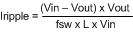
To find the worst case (lowest) current limit threshold, use the maximum input voltage and minimum current limit specification.
During high overcurrent conditions, such as output short circuit, the LM26003 device employs frequency foldback as a second level of protection. If the feedback voltage falls below the short circuit threshold of 0.9 V, operating frequency is reduced, thereby reducing average switch current. This is especially helpful in short circuit conditions, when inductor current can rise very high during the minimum on-time. Frequency reduction begins at 20% below the nominal frequency setting. The minimum operating frequency in foldback mode is 45 kHz (typical).
If the FB voltage falls below the frequency foldback threshold during frequency synchronized operation, the SYNC function is disabled. Operating frequency versus FB voltage in short circuit conditions is shown in the Typical Characteristics section.
Under conditions where the on-time is close to minimum (less than 200 ns typically), such as high input voltage and high switching frequency, the current limit may not function properly. This is because the current limit circuit cannot reduce the on-time below minimum which prevents entry into frequency foldback mode. There are two ways to ensure proper current limit and foldback operation under high input voltage conditions. First, the operating frequency can be reduced to increase the nominal on-time. Second, the inductor value can be increased to slow the current ramp and reduce the peak overcurrent.
8.3.4 Frequency Adjustment and Synchronization
The switching frequency of the LM26003 device can be adjusted between 150 kHz and 500 kHz using a single external resistor. This resistor is connected from the FREQ pin to ground as shown in the typical application. The resistor value can be calculated with the following empirically derived equation:
 Figure 12. Switching Frequency vs RFREQ
The switching frequency can also be synchronized to an external clock signal using the SYNC pin. The SYNC pin allows the operating frequency to be varied above and below the nominal frequency setting. The adjustment range is from 30% above nominal to 20% below nominal. External synchronization requires a 1.23-V minimum (typical) peak signal level at the SYNC pin. The FREQ resistor must always be connected to initialize the nominal operating frequency. The operating frequency is synchronized to the falling edge of the SYNC input. When SYNC goes low, the high-side switch turns on. This allows any duty-cycle to be used for the sync signal when synchronizing to a frequency higher than nominal. When synchronizing to a lower frequency, however, there is a minimum duty-cycle requirement for the SYNC signal, given in the equation below:
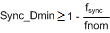
where
- fnom is the nominal switching frequency set by the FREQ resistor
- fsync is a square wave.
If the SYNC pin is not used, it must be pulled low for normal operation. A 10 kΩ pulldown resistor is recommended to protect against a missing sync signal. Although the LM26003 device is designed to operate at up to 500 kHz, maximum load current may be limited at higher frequencies due to increased temperature rise. See the Thermal Considerations and TSD section.
8.3.5 VBIAS
The VBIAS pin is used to bypass the internal regulator which provides the bias voltage to the LM26003 device. When the VBIAS pin is connected to a voltage greater than 3 V, the internal regulator automatically switches over to the VBIAS input. This reduces the current into VIN (Iq) and increases system efficiency. Using the VBIAS pin has the added benefit of reducing power dissipation within the device.
For most applications where 3 V < Vout < 10 V, VBIAS can be connected to VOUT. If not used, VBIAS should be tied to GND.
If VBIAS drops below 2.9 V (typical), the device automatically switches over to supply the internal bias voltage from Vin.
When the LM26003 device is powered with the circuit's output voltage through VBIAS, especially at low output voltages such as 3.3 V, output ripple noise can couple in through the Vbias pin causing some falling edge jitter on the switch node. To avoid this, additional bypassing close to the VBIAS pin with a low ESR capacitor can be implemented. The circuit diagram in Figure 16 shows this bypass capacitor C8.
8.3.6 Low VIN Operation and UVLO
The LM26003 device is designed to remain operational during short line transients when the input voltage may drop as low as 3.0 V. Minimum nominal operating input voltage is 4.0 V. Below this voltage, switch RDS(ON) increases, due to the lower gate drive voltage from VDD. The minimum voltage required at VDD is approximately 3.5 V for normal operation within specification.
VDD can also be used as a pullup voltage for functions such as PGOOD and FPWM. Note that if VDD is used externally, the pin is not recommended for loads greater than 1 mA.
If the input voltage approaches the nominal output voltage, the duty-cycle is maximized to hold up the output voltage. In this mode of operation, once the duty-cycle reaches its maximum, the LM26003 device can skip a maximum of seven off pulses, effectively increasing the duty-cycle and thus minimizing the dropout from input to output. Typical off-pulse skipping waveforms are shown in Figure 13.
 Figure 13. Off-Pulse Skipping Waveforms Vin = 3.5 V, Vnom = 3.3 V, fnom = 305 kHz
UVLO is sensed at both VIN and VDD, and is activated when either voltage falls below 2.96 V (typical). Although VDD is typically less than 200 mV below VIN, it will not discharge through VIN. Therefore when the VIN voltage drops rapidly, VDD may remain high, especially in sleep mode. For fast line voltage transients, using a larger capacitor at the VDD pin can help to hold off a UVLO shutdown by extending the VDD discharge time. By holding up VDD, a larger cap can also reduce the RDS(ON) (and dropout voltage) in low VIN conditions. Alternately, under heavy loading the VDD voltage can fall several hundred mV below VIN. In this case, UVLO may be triggered by VDD even though the VIN voltage is above the UVLO threshold.
When UVLO is activated the LM26003 device enters a standby state in which VDD remains charged. As input voltage and VDD voltage rise above 3.99 V (typical) the device will restart from soft-start mode.
8.3.7 PGOOD
A Power Good pin, PGOOD, is available to monitor the output voltage status. The pin is internally connected to an open-drain MOSFET, which remains open while the output voltage is within operating range. PGOOD goes low (low impedance to ground) when the output falls below 89% of nominal or EN is pulled low. When the output voltage returns to within 95% of nominal, as measured at the FB pin, PGOOD returns to a high state. For improved noise immunity, there is a 5-µs delay between the PGOOD threshold and the PGOOD pin going low.
8.4 Device Functional Modes
The LM26003 device has three basic operation modes: shutdown, sleep or light load operation and full operation. The part enters shutdown mode when the EN pin is pulled low. In this mode, the converter is disabled and the quiescent current is minimized. See the Enable section for more details.
The part enters sleep mode when the converter is active (EN high) and the output current is low. Sleep mode is activated as the COMP voltage naturally falls below a typical 0.6 V threshold in light load operation. When operating in sleep mode, the switching events of the converter are reduced in order to lower the current consumption of the system. Forcing the FPWM pin high will prevent sleep mode operation. Refer to Sleep Mode for details about operating in Sleep mode as well as entering and exiting sleep mode.
When the part in enabled and the output load is higher, the part will be in full PWM operation. In addition to these normal functioning modes, the LM26003 device has a frequency foldback operating mode which reduces the operating frequency to protect from short circuits. See Current Limitfor more details.
8.4.1 Enable
The LM26003 device provides a shutdown function via the EN pin to disable the device when the output voltage does not need to be maintained. EN is an analog level input with typically 180 mV of hysteresis. The device is active when the EN pin is above 1.18 V (typical) and in shutdown mode when EN is below this threshold. When EN goes high, the internal VDD regulator turns on and charges the VDD capacitor. When VDD reaches 3.9 V (typical), the soft-start pin begins to source current. In shutdown mode, the VDD regulator shuts down and total quiescent current is reduced to 10.8 µA (typical). Because the EN pin sources 4.85 µA (typical) of pullup current, this pin can be left open for always-on operation. When open, EN will be pulled up to VIN.
If EN is connected to VIN, it must be connected through a 10 kΩ resistor to limit noise spikes. EN can also be driven externally with a maximum voltage of 38 V or VIN + 15 V, whichever is lower.
8.4.2 Sleep Mode
In light load conditions, the LM26003 device automatically switches into sleep mode for improved efficiency. As loading decreases, the voltage at FB increases and the COMP voltage decreases. When the COMP voltage reaches the 0.6-V (typical) clamp threshold and the FB voltage rises 1% above nominal, sleep mode is enabled and switching stops. The regulator remains in sleep mode until the FB voltage falls to the reset threshold, at which point switching resumes. This 1% FB window limits the corresponding output ripple requirement to approximately 1% of nominal output voltage. The sleep cycle will repeat until load current is increased. Figure 14 shows typical switching and output voltage waveforms in sleep mode.
 Figure 14. Sleep Mode Waveforms 25-mA Load, Vin = 12 V
In sleep mode, quiescent current is reduced to less than 40 µA (typical) when not switching. The DC sleep mode threshold can roughly be calculated according to the equation below:
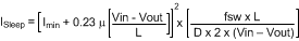
where
- Imin = Ilim/16 (4.7A/16 typically)
- D = duty-cycle, defined as (Vout + Vdiode)/Vin.
When load current increases above this limit, the LM26003 device is forced back into PWM operation. The sleep mode threshold varies with frequency, inductance, and duty-cycle as shown in Figure 15.
 Figure 15. Sleep Mode Threshold vs Vin Vout = 3.3 V
Below the sleep threshold, decreasing load current results in longer sleep cycles, which can be quantified as shown below:
where
- Dwake is the percentage of time awake when the load current is below the sleep threshold.
Sleep mode combined with low IQ operation minimizes the input supply current. Input supply current in sleep mode can be calculated based on the wake duty cycle, as shown below:
Where IQG is the gate drive current, calculated as:
And Io is the sum of Iload, Ibias, and current through the feedback resistors.
Because this calculation applies only to sleep mode, use the Iq_Sleep_VB and IBIAS_SLEEP values from the Electrical Characteristics. If VBIAS is connected to ground, use the same equation with Ibias equal to zero and Iq_Sleep_VDD.