SNVS576F August 2008 – February 2015 LM26003 , LM26003-Q1
PRODUCTION DATA.
- 1 Features
- 2 Applications
- 3 Description
- 4 Typical Application Circuit
- 5 Revision History
- 6 Pin Configuration and Functions
- 7 Specifications
- 8 Detailed Description
- 9 Application and Implementation
- 10Power Supply Recommendations
- 11Layout
- 12Device and Documentation Support
- 13Mechanical, Packaging, and Orderable Information
Package Options
Mechanical Data (Package|Pins)
- PWP|20
Thermal pad, mechanical data (Package|Pins)
- PWP|20
Orderable Information
6 Pin Configuration and Functions
20-Pin
TSSOP Package
Top View
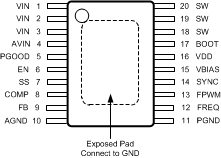
Pin Functions
| PIN | I/O | DESCRIPTION | |
|---|---|---|---|
| NAME | NO. | ||
| VIN | 1 | I | Power supply input for high side FET |
| VIN | 2 | I | Power supply input for high side FET |
| VIN | 3 | I | Power supply input for high side FET |
| AVIN | 4 | I | Power supply input for IC supply |
| PGOOD | 5 | O | Power Good pin. An open-drain output which goes high when the output voltage is greater than 92% of nominal. |
| EN | 6 | I | Enable is an analog level input pin. When pulled below 0.8 V, the device enters shutdown mode. |
| SS | 7 | I | Soft-start pin. Connect a capacitor from this pin to GND to set the soft-start time. |
| COMP | 8 | I | Compensation pin. Connect to a resistor capacitor pair to compensate the control loop. |
| FB | 9 | I | Feedback pin. Connect to a resistor divider between VOUT and GND to set output voltage. |
| AGND | 10 | GND | Analog GND as IC reference |
| PGND | 11 | GND | Power GND is GND for the switching stage of the regulator |
| FREQ | 12 | O | Frequency adjust pin. Connect a resistor from this pin to GND to set the operating frequency. |
| FPWM | 13 | I | FPWM is a logic level input pin. For normal operation, connect to GND. When pulled high, sleep mode operation is disabled. |
| SYNC | 14 | I | Frequency synchronization pin. Connect to an external clock signal for synchronized operation. SYNC must be pulled low for non-synchronized operation. |
| VBIAS | 15 | I | Connect to an external 3-V or greater supply to bypass the internal regulator for improved efficiency. If not used, VBIAS should be tied to GND. |
| VDD | 16 | O | The output of the internal regulator. Bypass with a minimum 1.0-µF capacitor. |
| BOOT | 17 | I | Bootstrap capacitor pin. Connect a 0.1-µF minimum ceramic capacitor from this pin to SW to generate the gate drive bootstrap voltage. |
| SW | 18 | O | Switch pin. The source of the internal N-channel switch. |
| SW | 19 | O | Switch pin. The source of the internal N-channel switch. |
| SW | 20 | O | Switch pin. The source of the internal N-channel switch. |
| EP | EP | GND | Exposed Pad thermal connection. Connect to GND. |