SNVS576F August 2008 – February 2015 LM26003 , LM26003-Q1
PRODUCTION DATA.
- 1 Features
- 2 Applications
- 3 Description
- 4 Typical Application Circuit
- 5 Revision History
- 6 Pin Configuration and Functions
- 7 Specifications
- 8 Detailed Description
- 9 Application and Implementation
- 10Power Supply Recommendations
- 11Layout
- 12Device and Documentation Support
- 13Mechanical, Packaging, and Orderable Information
Package Options
Mechanical Data (Package|Pins)
- PWP|20
Thermal pad, mechanical data (Package|Pins)
- PWP|20
Orderable Information
9 Application and Implementation
NOTE
Information in the following applications sections is not part of the TI component specification, and TI does not warrant its accuracy or completeness. TI’s customers are responsible for determining suitability of components for their purposes. Customers should validate and test their design implementation to confirm system functionality.
9.1 Application Information
The LM26003 is a switching regulator designed for the high-efficiency requirements of applications with standby modes.
9.2 Typical Application
The following sections detail the design of a typical buck converter with sleep mode operation enabled (FPWM low). Figure 16 shows a complete typical application schematic. The components have been selected based on the design criteria given in the following sections.
 Figure 16. Example Circuit 3A, 300 kHz
9.2.1 Design Requirements
The following parameters are needed to properly design the application and size the components:
Table 1. Design Parameters
| PARAMETERS | VALUES |
|---|---|
| Vout | Output voltage |
| Vin min | Maximum input voltage |
| Vin max | Minimum input voltage |
| Iout max | Maximum output current |
| Fsw | Switching Frequency |
| Fbw | Bandwidth of the converter |
9.2.2 Detailed Design Procedure
Table 2. Bill of Materials
| REFERENCE NUMBER | MANUFACTURER | PART NUMBER |
|---|---|---|
| C7 | Nippon Chemi-Con | APXE6R3ARA121ME61G |
| C9 | TDK | C4532X7R1H685M |
| C10 | Panasonic | EEE-FK1J101P |
| D1 | Central Semiconductor | CMSH 5-40 |
| L1 | Wurth | 744770115 |
9.2.2.1 Setting Output Voltage
The output voltage is set by the ratio of a voltage divider at the FB pin as shown in the typical application. The resistor values can be determined by the following equation:

where
- Vfb = 1.236 V typically.
A maximum value of 150 kΩ is recommended for the sum of R1 and R2.
As input voltage decreases towards the nominal output voltage, the LM26003 device can skip up to seven off-pulses as described in the Low VIN Operation and UVLO section. In low output voltage applications, if the on-time reaches TonMIN, the device will skip on-pulses to maintain regulation. There is no limit to the number of pulses that are skipped. In this mode of operation, however, output ripple voltage may increase slightly.
9.2.2.2 Inductor
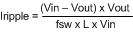
The output inductor should be selected based on inductor ripple current. The amount of inductor ripple current compared to load current, or ripple content, is defined as Iripple/Iload. Ripple content should be less than 40%. Inductor ripple current, Iripple, can be calculated as shown below:
Larger ripple content increases losses in the inductor and reduces the effective current limit.
Larger inductance values result in lower output ripple voltage and higher efficiency, but a slightly degraded transient response. Lower inductance values allow for smaller case size, but the increased ripple lowers the effective current limit threshold.
Remember that inductor value also affects the sleep mode threshold as shown in Figure 15.
When choosing the inductor, the saturation current rating must be higher than the maximum peak inductor current and the RMS current rating should be higher than the maximum load current. Peak inductor current, Ipeak, is calculated as:
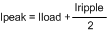
For example, at a maximum load of 3 A and a ripple content of 10%, peak inductor current is equal to 3.15 A which is safely at the minimum current limit of 3.15 A. By increasing the inductor size, ripple content and peak inductor current are lowered, which increases the current limit margin.
The size of the output inductor can also be determined using the desired output ripple voltage, Vrip. The equation to determine the minimum inductance value based on Vrip is as follows:
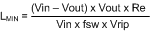
Where Re is the ESR of the output capacitors, and Vrip is a peak-to-peak value. This equation assumes that the output capacitors have some amount of ESR. It does not apply to ceramic output capacitors.
If this method is used, ripple content should still be verified to be less than 40% and that the peak currents do not exceed the minimum current threshold.
9.2.2.3 Output Capacitor
The primary criterion for selecting an output capacitor is equivalent series resistance, or ESR.
ESR (Re) can be selected based on the requirements for output ripple voltage and transient response. Once an inductor value has been selected, ripple voltage can be calculated for a given Re using the equation above for LMIN. Lower ESR values result in lower output ripple.
Re can also be calculated from the following equation:

where
- ΔVt is the allowed voltage excursion during a load transient
- ΔIt is the maximum expected load transient.
If the total ESR is too high, the load transient requirement cannot be met, no matter how large the output capacitance.
If the ESR criteria for ripple voltage and transient excursion cannot be met, more capacitors should be used in parallel.
For non-ceramic capacitors, the minimum output capacitance is of secondary importance, and is determined only by the load transient requirement.
If there is not enough capacitance, the output voltage excursion will exceed the maximum allowed value even if the maximum ESR requirement is met. The minimum capacitance is calculated as follows:
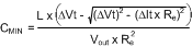
It is assumed the total ESR, Re, is no greater than ReMAX. Also, it is assumed that L has already been selected.
Generally speaking, the output capacitance requirement decreases with Re, ΔIt, and L. A typical value greater than 120 µF works well for most applications.
9.2.2.4 Input Capacitor
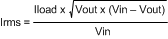
In a switching converter, very fast switching pulse currents are drawn from the input rail. Therefore, input capacitors are required to reduce noise, EMI, and ripple at the input to the LM26003 device. Capacitors must be selected that can handle both the maximum ripple RMS current at highest ambient temperature as well as the maximum input voltage. The equation for calculating the RMS input ripple current is shown below:
For noise suppression, a ceramic capacitor in the range of 1.0 µF to 10 µF should be placed as close as possible to the PVIN pin. For the AVIN pin also some decoupling is necessary. It is very important that the pin is decoupled with such a capacitor close to the AGND pin and the GND pin of the IC to avoid switching noise to couple into the IC. Also some RC input filtering can be implemented using a small resistor between PVIN and AVIN. In Figure 16 the resistor value of R7 is selected to be 0Ω but can be increased to filter with different time constants depending on the capacitor value used. When using a R7 resistor, keep in mind that the resistance will increase the minimum input voltage threshold due to the voltage drop across the resistor.
The PVIN decoupling should be implemented in a way to minimize the trace length between the Cin capacitor gnd and the Schottky diode gnd. A larger, high ESR input capacitor should also be used. This capacitor is recommended for damping input voltage spikes during power-on and for holding up the input voltage during transients. In low input voltage applications, line transients may fall below the UVLO threshold if there is not enough input capacitance. Both tantalum and electrolytic type capacitors are suitable for the bulk capacitor. However, large tantalums may not be available for high input voltages and their working voltage must be derated by at least 2X.
9.2.2.5 Bootstrap
The drive voltage for the internal switch is supplied via the BOOT pin. This pin must be connected to a ceramic capacitor, Cboot, from the switch node, shown as C6 in the typical application. The LM26003 device provides the VDD voltage internally, so no external diode is needed. A maximum value of 0.1 µF is recommended for Cboot. Values smaller than 0.022 µF may result in insufficient hold up time for the drive voltage and increased power dissipation.
During low Vin operation, when the on-time is extended, the bootstrap capacitor is at risk of discharging. If the Cboot capacitor is discharged below approximately 2.5 V, the LM26003 device enters a high frequency re-charge mode. The Cboot cap is re-charged via the synchronous FET shown in the block diagram. Switching returns to normal when the Cboot cap has been recharged.
9.2.2.6 Catch Diode
When the internal switch is off, output current flows through the catch diode. Alternately, when the switch is on, the diode sees a reverse voltage equal to Vin. Therefore, the important parameters for selecting the catch diode are peak current and peak inverse voltage. The average current through the diode is given by:
where
- D is the duty-cycle, defined as Vout/Vin.
The catch diode conducts the largest currents during the lowest duty-cycle. Therefore IDAVE should be calculated assuming maximum input voltage. The diode should be rated to handle this current continuously. For overcurrent or short-circuit conditions, the catch diode should be rated to handle peak currents equal to the peak current limit.
The peak inverse voltage rating of the diode must be greater than maximum input voltage.
A Schottky diode must be used. It's low forward voltage maximizes efficiency and BOOT voltage, while also protecting the SW pin against large negative voltage spikes.
When selecting the catch diode for high efficiency low output load applications, select a Schottky diode with low reverse leakage current. Also keep in mind that the reverse leakage current of a Schottky diode increases with temperature and with reverse voltage. Reverse voltage equals roughly the input voltage in a buck converter. At hot, the diode reverse leakage current may be larger than the current consumption of the LM26003 device.
9.2.2.7 Compensation
The purpose of loop compensation is to ensure stable operation while maximizing dynamic performance. Stability can be analyzed with loop gain measurements, while dynamic performance is analyzed with both loop gain and load transient response. Loop gain is equal to the product of control-output transfer function (power stage) and the feedback transfer function (the compensation network).
For stability purposes, our target is to have a loop gain slope that is –20dB/decade from a very low frequency to beyond the crossover frequency. Also, the crossover frequency should not exceed one-fifth of the switching frequency, that is, 60 kHz in the case of 300 kHz switching frequency.
For dynamic purposes, the higher the bandwidth, the faster the load transient response. The downside to high bandwidth is that it increases the regulators susceptibility to board noise which ultimately leads to excessive falling edge jitter of the switch node voltage.
A large DC gain means high DC regulation accuracy (that is, DC voltage changes little with load or line variations).
To achieve this loop gain, the compensation components should be set according to the shape of the control-output bode plot. A typical plot is shown in Figure 17.
 Figure 17. Control-Output Transfer Function
The control-output transfer function consists of one pole (fp), one zero (fz), and a double pole at fn (half the switching frequency).
Referring to Figure 17, the following should be done to create a –20dB/decade roll-off of the loop gain:
- Place a pole at 0Hz (fpc)
- Place a zero at fp (fzc)
- Place a second pole at fz (fpc1)
The resulting feedback (compensation) bode plot is shown below in Figure 18. Adding the control-output response to the feedback response will then result in a nearly continuous -20db/decade slope.
 Figure 18. Feedback Transfer Function
The control-output corner frequencies can be determined approximately by the following equations:
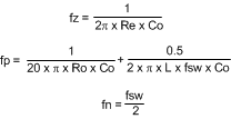
where
- Co is the output capacitance
- Ro is the load resistance
- Re is the output capacitor ESR
- fsw is the switching frequency.
The effects of slope compensation and current sense gain are included in this equation. However, the equation is an approximation intended to simplify loop compensation calculations.
Since fp is determined by the output network, it shifts with loading. Determine the range of frequencies (fpmin/max) across the expected load range. Then determine the compensation values as described below and shown in Figure 19.
 Figure 19. Compensation Network
- The compensation network automatically introduces a low frequency pole (fpc), which is close to 0 Hz.
- Once the fp range is determined, R5 should be calculated using:
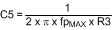
- Next, place a zero (fzc) near fp using C5. C5 can be determined with the following equation:
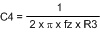
- A second pole (fpc1) can also be placed at fz. This pole can be created with a single capacitor, C4. The minimum value for this capacitor can be calculated by:
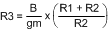
Where B is the desired feedback gain in v/v between fp and fz, and gm is the transconductance of the error amplifier. A gain value around 10 dB (3.3 V/V) is generally a good starting point. Bandwidth increases with increasing values of R3.
The selected value of C5 should place fzc within a decade above or below fpmax and not less than fpmin. A higher C5 value (closer to fpmin) generally provides a more stable loop, but too high a value will slow the transient response time. Conversely, a smaller C5 value will result in a faster transient response, but lower phase margin.
C4 may not be necessary in all applications. However if the operating frequency is being synchronized below the nominal frequency, C4 is recommended. Although it is not required for stability, C4 is very helpful in suppressing noise.
A phase lead capacitor can also be added to increase the phase and gain margins. The phase lead capacitor is most helpful for high input voltage applications or when synchronizing to a frequency greater than nominal. This capacitor, shown as C11 in Figure 19, should be placed in parallel with the top feedback resistor, R1.
C11 introduces an additional zero and pole to the compensation network. These frequencies can be calculated as shown below:
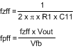
A phase lead capacitor will boost loop phase around the region of the zero frequency, fzff. fzff should be placed somewhat below the fpz1 frequency set by C4. However, if C11 is too large, it will have no effect.
9.2.3 Application Curves
Refer to Typical Characteristics.

