SNVSB73 September 2018 LM2735-Q1
PRODUCTION DATA.
- 1 Features
- 2 Applications
- 3 Description
- 4 Revision History
- 5 Pin Configuration and Functions
- 6 Specifications
- 7 Detailed Description
-
8 Application and Implementation
- 8.1 Application Information
- 8.2
Typical Applications
- 8.2.1 LM2735X-Q1 SOT-23 Design Example 1
- 8.2.2 LM2735Y-Q1 SOT-23 Design Example 2
- 8.2.3 LM2735X-Q1 WSON Design Example 3
- 8.2.4 LM2735Y-Q1 WSON Design Example 4
- 8.2.5 LM2735X-Q1 SOT-23 Design Example 6
- 8.2.6 LM2735Y-Q1 SOT-23 Design Example 7
- 8.2.7 LM2735X-Q1 SOT-23 Design Example 8
- 8.2.8 LM2735Y-Q1 SOT-23 Design Example 9
- 8.2.9 LM2735X-Q1 WSON Design Example 10
- 8.2.10 LM2735Y-Q1 WSON Design Example 11
- 8.2.11 LM2735X-Q1 WSON SEPIC Design Example 12
- 8.2.12 LM2735X-Q1 SOT-23 LED Design Example 14
- 8.2.13 LM2735Y-Q1 WSON FlyBack Design Example 15
- 8.2.14 LM2735X-Q1 SOT-23 LED Design Example 16 VRAIL > 5.5 V Application
- 8.2.15 LM2735X-Q1 SOT-23 LED Design Example 17 Two-Input Voltage Rail Application
- 8.2.16 SEPIC Converter
- 9 Power Supply Recommendations
- 10Layout
- 11Device and Documentation Support
- 12Mechanical, Packaging, and Orderable Information
Package Options
Mechanical Data (Package|Pins)
Thermal pad, mechanical data (Package|Pins)
Orderable Information
8.2.1.2.2 Inductor Selection
The duty cycle (D) can be approximated quickly using the ratio of output voltage (VO) to input voltage (VIN):

Therefore:

Power losses due to the diode (D1) forward voltage drop, the voltage drop across the internal NMOS switch, the voltage drop across the inductor resistance (RDCR), and switching losses must be included to calculate a more accurate duty cycle (see Calculating Efficiency, and Junction Temperature for a detailed explanation). A more accurate formula for calculating the conversion ratio is:

where
- η equals the efficiency of the LM2735-Q1 application.
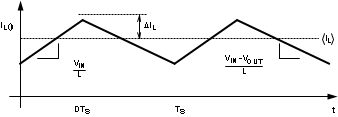
The inductor value determines the input ripple current. Lower inductor values decrease the size of the inductor, but increase the input ripple current. An increase in the inductor value decreases the input ripple current.
 Figure 19. Inductor Current
A good design practice is to design the inductor to produce 10% to 30% ripple of maximum load. From the previous equations, the inductor value is then obtained.

where
- 1/TS = FSW = switching frequency
Ensure that the minimum current limit (2.1 A) is not exceeded, so the peak current in the inductor must be calculated. The peak current (ILPK ) in the inductor is calculated by:
or
When selecting an inductor, make sure that it is capable of supporting the peak input current without saturating. Inductor saturation results in a sudden reduction in inductance and prevent the regulator from operating correctly. Because of the speed of the internal current limit, the peak current of the inductor need only be specified for the required maximum input current. For example, if the designed maximum input current is 1.5 A and the peak current is 1.75 A, then the inductor should be specified with a saturation current limit of >1.75 A. There is no need to specify the saturation or peak current of the inductor at the 3-A typical switch current-limit.
Because of the operating frequency of the LM2735-Q1, ferrite based inductors are preferred to minimize core losses. This presents little restriction since the variety of ferrite-based inductors is huge. Lastly, inductors with lower series resistance (DCR) provides better operating efficiency. For recommended inductors, see the following design examples.