SNVS276I April 2004 – February 2019 LM2743
PRODUCTION DATA.
- 1 Features
- 2 Applications
- 3 Description
- 4 Revision History
- 5 Pin Configuration and Functions
- 6 Specifications
- 7 Detailed Description
- 8 Application and Implementation
- 9 Power Supply Recommendations
- 10Layout
- 11Device and Documentation Support
- 12Mechanical, Packaging, and Orderable Information
Package Options
Mechanical Data (Package|Pins)
- PW|14
Thermal pad, mechanical data (Package|Pins)
Orderable Information
7.3.10 Current Limit
Current limit is realized by sensing the voltage across the low-side MOSFET while it is on. The RDS(ON) of the MOSFET is a known value; hence the current through the MOSFET can be determined as:
The current through the low-side MOSFET while it is on is also the falling portion of the inductor current. The current limit threshold is determined by an external resistor, RCS, connected between the switching node and the ISEN pin. A constant current of 40 µA is forced through RCS, causing a fixed voltage drop. This fixed voltage is compared against VDS and if the latter is higher, the current limit of the chip has been reached. To obtain a more accurate value for RCS you must consider the operating values of RDS(ON) and ISEN-TH at their operating temperatures in your application and the effect of slight parameter differences from part to part. RCS can be found by using the following equation using the RDS(ON) value of the low side MOSFET at it's expected hot temperature and the absolute minimum value expected over the full temperature range for the for the ISEN-TH which is 25 µA:
For example, a conservative 15-A current limit in a 10-A design with a minimum RDS(ON) of 10 mΩ would require a 6-kΩ resistor. To prevent the ISEN pin from sinking too much current when the switch node goes above 9.5 V, the value of the current limit setting resistor RCS should not be too low. The criterion is as follows,

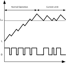
where the 10 mA is the maximum current ISEN pin is allowed to sink. For example if VIN = 13.2 V, the minimum value of RCS is 370 Ω. Because current sensing is done across the low-side MOSFET, no minimum high-side on-time is necessary. The LM2743 enters current limit mode if the inductor current exceeds the current limit threshold at the point where the high-side MOSFET turns off and the low-side MOSFET turns on. (The point of peak inductor current, see Figure 28). Note that in normal operation mode the high-side MOSFET always turns on at the beginning of a clock cycle. In current limit mode, by contrast, the high-side MOSFET on-pulse is skipped. This causes inductor current to fall. Unlike a normal operation switching cycle, however, in a current limit mode switching cycle the high-side MOSFET will turn on as soon as inductor current has fallen to the current limit threshold. The LM2743 will continue to skip high-side MOSFET pulses until the inductor current peak is below the current limit threshold, at which point the system resumes normal operation.
 Figure 28. Current Limit Threshold
 Unlike a high-side MOSFET current sensing scheme, which limits the peaks of inductor current, low-side current sensing is only allowed to limit the current during the converter off-time, when inductor current is falling. Therefore in a typical current limit plot the valleys are normally well defined, but the peaks are variable, according to the duty cycle. The PWM error amplifier and comparator control the off-pulse of the high-side MOSFET, even during current limit mode, meaning that peak inductor current can exceed the current limit threshold. Assuming that the output inductor does not saturate, the maximum peak inductor current during current limit mode can be calculated with the following equation:

Where TSW is the inverse of switching frequency fSW. The 200 ns term represents the minimum off-time of the duty cycle, which ensures enough time for correct operation of the current sensing circuitry.
In order to minimize the time period in which peak inductor current exceeds the current limit threshold, the IC also discharges the soft-start capacitor through a fixed 90-µA sink. The output of the LM2743 internal error amplifier is limited by the voltage on the soft-start capacitor. Hence, discharging the soft-start capacitor reduces the maximum duty cycle D of the controller. During severe current limit this reduction in duty cycle will reduce the output voltage if the current limit conditions last for an extended time. Output inductor current will be reduced in turn to a flat level equal to the current limit threshold. The third benefit of the soft-start capacitor discharge is a smooth, controlled ramp of output voltage when the current limit condition is cleared.