SNVS276I April   2004  – February 2019 LM2743

PRODUCTION DATA.  

  1. Features
  2. Applications
  3. Description
    1.     Device Images
      1.      Typical Application Diagram
  4. Revision History
  5. Pin Configuration and Functions
    1.     Pin Functions
  6. Specifications
    1. 6.1 Absolute Maximum Ratings
    2. 6.2 ESD Ratings
    3. 6.3 Recommended Operating Conditions
    4. 6.4 Thermal Information
    5. 6.5 Electrical Characteristics
    6. 6.6 Typical Characteristics
  7. Detailed Description
    1. 7.1 Overview
    2. 7.2 Functional Block Diagram
    3. 7.3 Feature Description
      1. 7.3.1  Start Up and Soft-Start
      2. 7.3.2  Normal Operation
      3. 7.3.3  Tracking a Voltage Level
      4. 7.3.4  Tracking Voltage Slew Rate
      5. 7.3.5  Sequencing
      6. 7.3.6  SD Pin Impedance
      7. 7.3.7  MOSFET Gate Drivers
      8. 7.3.8  Power Good Signal
      9. 7.3.9  UVLO
      10. 7.3.10 Current Limit
      11. 7.3.11 Foldback Current Limit
    4. 7.4 Device Functional Modes
      1. 7.4.1 Shutdown
  8. Application and Implementation
    1. 8.1 Application Information
    2. 8.2 Typical Applications
      1. 8.2.1 Synchronous Buck Converter Typical Application using LM2743
        1. 8.2.1.1 Design Requirements
        2. 8.2.1.2 Detailed Design Procedure
          1. 8.2.1.2.1 Custom Design With WEBENCH® Tools
          2. 8.2.1.2.2 Duty Cycle Calculation
          3. 8.2.1.2.3 Input Capacitor
          4. 8.2.1.2.4 Output Inductor
          5. 8.2.1.2.5 Output Capacitor
          6. 8.2.1.2.6 MOSFETs
          7. 8.2.1.2.7 Support Components
          8. 8.2.1.2.8 Control Loop Compensation
          9. 8.2.1.2.9 Efficiency Calculations
        3. 8.2.1.3 Application Curves
      2. 8.2.2 Example Circuit 1
        1. 8.2.2.1 Design Requirements
        2. 8.2.2.2 Detailed Design Procedure
        3. 8.2.2.3 Bill of Materials
      3. 8.2.3 Example Circuit 2
        1. 8.2.3.1 Design Requirements
        2. 8.2.3.2 Detailed Design Procedure
        3. 8.2.3.3 Bill of Materials
      4. 8.2.4 Example Circuit 3
        1. 8.2.4.1 Design Requirements
        2. 8.2.4.2 Detailed Design Procedure
        3. 8.2.4.3 Bill of Materials
  9. Power Supply Recommendations
  10. 10Layout
    1. 10.1 Layout Guidelines
    2. 10.2 Layout Example
  11. 11Device and Documentation Support
    1. 11.1 Device Support
      1. 11.1.1 Development Support
        1. 11.1.1.1 Custom Design With WEBENCH® Tools
    2. 11.2 Receiving Notification of Documentation Updates
    3. 11.3 Community Resources
    4. 11.4 Trademarks
    5. 11.5 Electrostatic Discharge Caution
    6. 11.6 Glossary
  12. 12Mechanical, Packaging, and Orderable Information

Package Options

Mechanical Data (Package|Pins)
Thermal pad, mechanical data (Package|Pins)
Orderable Information

Foldback Current Limit

In the case where extra protection is used to help an output short condition, a current foldback resistor (RCLF) should be considered, see Figure 29. First select the percentage of current limit foldback (PLIM):

Equation 12. PLIM = ILIM x P

where P is a ratio between 0 and 1.
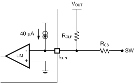
LM2743 20095295.gifFigure 29. Foldback Current Limit Circuit

Obtain the RCS with the following equation:

Equation 13. LM2743 20095293.gif

where ISEN = 40 μA. If the switch node goes above 9.5 V the following criterion must be satisfied:

Equation 14. LM2743 20095292.gif

The equation for calculating the foldback resistance value is:

Equation 15. LM2743 20095294.gif