SNVSAH6C June 2018 – May 2021 LM2775-Q1
PRODUCTION DATA
- 1 Features
- 2 Applications
- 3 Description
- 4 Revision History
- 5 Pin Configuration and Functions
- 6 Specifications
- 7 Detailed Description
- 8 Application and Implementation
- 9 Power Supply Recommendations
- 10Layout
- 11Device and Documentation Support
- 12Mechanical, Packaging, and Orderable Information
Package Options
Mechanical Data (Package|Pins)
- DSG|8
Thermal pad, mechanical data (Package|Pins)
- DSG|8
Orderable Information
8.2.2.5 Output Capacitor and Output Voltage Ripple
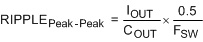
The output capacitor in the LM2775-Q1 circuit (COUT) directly impacts the magnitude of output voltage ripple. Other prominent factors also affecting output voltage ripple include input voltage, output current, and flying capacitance. One important generalization can be made: increasing (decreasing) the output capacitance results in a proportional decrease (increase) in output voltage ripple. A simple approximation of output ripple is determined by calculating the amount of voltage droop that occurs when the output of the LM2775-Q1 is not being driven. This occurs during the charge phase (φ1). During this time, the load is driven solely by the charge on the output capacitor. The magnitude of the ripple thus follows the basic discharge equation for a capacitor (I = C × dV/dt), where discharge time is one-half the switching period, or 0.5/FSW (see Equation 6).
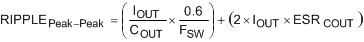
A more thorough and accurate examination of factors that affect ripple requires including effects of phase non-overlap times and output capacitor ESR. In order for the LM2775-Q1 to operate properly, the two phases of operation must never coincide. (If this were to happen all switches would be closed simultaneously, shorting input, output, and ground). Thus, non-overlap time is built into the clocks that control the phases. Because the output is not being driven during the non-overlap time, this time should be accounted for in calculating ripple. Actual output capacitor discharge time is approximately 60% of a switching period, or 0.6/FSW (see Equation 7).
In typical high-current applications, a 10-µF, 10-V low-ESR ceramic output capacitor is recommended. Different output capacitance values can be used to reduce ripple, shrink the solution size, and/or cut the cost of the solution. But changing the output capacitor may also require changing the flying capacitor and/or input capacitor to maintain good overall circuit performance. If a small output capacitor is used and PFM mode is enabled, the output ripple can become large during the transition between PFM mode and constant switching. To prevent toggling, a 2-µF capacitance is recommended. For example, a 10-µF, 10-V output capacitor in a 0402 case size will typically only have 2-µF capacitance when biased to 5 V.
High ESR in the output capacitor increases output voltage ripple. If a ceramic capacitor is used at the output, this is usually not a concern because the ESR of a ceramic capacitor is typically very low and has only a minimal impact on ripple magnitudes. If a different capacitor type with higher ESR is used (tantalum, for example), the ESR could result in high ripple. To eliminate this effect, the net output ESR can be significantly reduced by placing a low-ESR ceramic capacitor in parallel with the primary output capacitor. The low ESR of the ceramic capacitor is in parallel with the higher ESR, resulting in a low net ESR based on the principles of parallel resistance reduction.