SNVS416C November 2005 – February 2016 LM27951
PRODUCTION DATA.
- 1 Features
- 2 Applications
- 3 Description
- 4 Revision History
- 5 Pin Configuration and Functions
- 6 Specifications
- 7 Detailed Description
- 8 Application and Implementation
- 9 Power Supply Recommendations
- 10Layout
- 11Device and Documentation Support
- 12Mechanical, Packaging, and Orderable Information
Package Options
Mechanical Data (Package|Pins)
- NHK|14
Thermal pad, mechanical data (Package|Pins)
Orderable Information
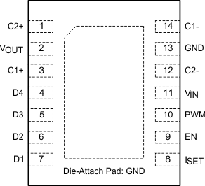
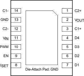
5 Pin Configuration and Functions
NHK Package
14-Pin WSON
Top View

NHK Package
14-Pin WSON
Bottom View

Pin Functions
| PIN | TYPE | DESCRIPTION | |
|---|---|---|---|
| NUMBER | NAME | ||
| 1 | C2+ | Power | Flying capacitor C2 connection |
| 2 | VOUT | Power | Pre-regulated charge-pump output |
| 3 | C1+ | Power | Flying capacitor C1 connection |
| 4 | D4 | Output | Regulated current source output |
| 5 | D3 | Output | Regulated current source output |
| 6 | D2 | Output | Regulated current source output |
| 7 | D1 | Output | Regulated current source output |
| 8 | ISET | Input | Current set input. Placing a resistor (RSET) between this pin and GND sets the LED current for all the LEDs. LED current = 200 × (1.25 V / RSET). |
| 9 | EN | Input | Enable logic input pin. Logic low = shutdown; Logic high = enabled. There is a 150-kΩ (typical) resistor connected internally between the EN pin and GND. |
| 10 | PWM | Input | Current source modulation logic input pin. Logic low = Off; Logic high = On. Applying a pulse width modulated (PWM) signal to this pin allows the regulated current sources to be modulated without shutting down the internal charge pump and the VOUT node. |
| 11 | VIN | Input | Input supply: 2.8 V to 5.5 V |
| 12 | C2- | Power | Flying capacitor C2 connection |
| 13 | GND | Ground | Power supply ground connection |
| 14 | C1- | Power | Flying capacitor C1 connection |