SNVS416C November 2005 – February 2016 LM27951
PRODUCTION DATA.
- 1 Features
- 2 Applications
- 3 Description
- 4 Revision History
- 5 Pin Configuration and Functions
- 6 Specifications
- 7 Detailed Description
- 8 Application and Implementation
- 9 Power Supply Recommendations
- 10Layout
- 11Device and Documentation Support
- 12Mechanical, Packaging, and Orderable Information
Package Options
Mechanical Data (Package|Pins)
- NHK|14
Thermal pad, mechanical data (Package|Pins)
Orderable Information
6 Specifications
6.1 Absolute Maximum Ratings
over operating free-air temperature range (unless otherwise noted)(1)(2)| MIN | MAX | UNIT | ||
|---|---|---|---|---|
| VIN | –0.3 | 6 | V | |
| EN, PWM | –0.3 | VIN + 0.3(3) | V | |
| Continuous power dissipation | Internally limited | |||
| Junction temperature, TJ-MAX-ABS | 150 | °C | ||
| Lead temperature (Soldering, 5 sec.) | 260 | °C | ||
| Storage temperature, Tstg | –65 | 150 | °C | |
(1) Stresses beyond those listed under Absolute Maximum Ratings may cause permanent damage to the device. These are stress ratings only, which do not imply functional operation of the device at these or any other conditions beyond those indicated under Recommended Operating Conditions. Exposure to absolute-maximum-rated conditions for extended periods may affect device reliability.
(2) If Military/Aerospace specified devices are required, contact the Texas Instruments Sales Office / Distributors for availability and specifications.
(3) Maximum value is 6 V.
(4) Internal thermal shutdown circuitry protects the device from permanent damage. Thermal shutdown engages at(4) TJ =150°C (typical) and disengages at TJ = 140°C (typical).
6.2 ESD Ratings
| VALUE | UNIT | |||
|---|---|---|---|---|
| V(ESD) | Electrostatic discharge | Human-body model (HBM), per ANSI/ESDA/JEDEC JS-001(1) | ±2000 | V |
(1) JEDEC document JEP155 states that 500-V HBM allows safe manufacturing with a standard ESD control process.
6.3 Recommended Operating Conditions
over operating free-air temperature range (unless otherwise noted)(1)(2)(3)| MIN | NOM | MAX | UNIT | ||
|---|---|---|---|---|---|
| Inpu voltage, VIN | 2.8 | 5.5 | V | ||
| LED voltage | 2.5 | 3.9 | V | ||
| Junction temperature, TJ | –40 | 115 | °C | ||
| Ambient temperature, TA | –40 | 85 | °C | ||
(1) All voltages are with respect to the potential at the GND pin.
(2) Minimum and maximum limits are ensured by design, test, or statistical analysis. Typical numbers are not ensured, but do represent the most likely norm.
(3) In applications where high power dissipation and/or poor package thermal resistance is present, the maximum ambient temperature may have to be derated. Maximum ambient temperature (TA-MAX) is dependent on the maximum operation junction temperature (TJ-MAX-OP = 115°C), the maximum power dissipation of the device in the application (PD-MAX), and the junction-to ambient thermal resistance of the part/package in the application (RθJA), as given by the equation: TA-MAX = TJ-MAX-OP – (RθJA × PD-MAX).
6.4 Thermal Information
| THERMAL METRIC(1) | LM27951 | UNIT | |
|---|---|---|---|
| NHK (WSON) | |||
| 14 PINS | |||
| RθJA | Junction-to-ambient thermal resistance | 42.5 | °C/W |
| RθJC(top) | Junction-to-case (top) thermal resistance | 33.3 | °C/W |
| RθJB | Junction-to-board thermal resistance | 14.1 | °C/W |
| ψJT | Junction-to-top characterization parameter | 0.5 | °C/W |
| ψJB | Junction-to-board characterization parameter | 14.1 | °C/W |
| RθJC(bot) | Junction-to-case (bottom) thermal resistance | 6.1 | °C/W |
(1) For more information about traditional and new thermal metrics, see the Semiconductor and IC Package Thermal Metrics application report, SPRA953.
6.5 Electrical Characteristics
Unless otherwise noted, typical limits are for TA = 25°C, and minimum and maximum limits apply over the full operating temperature (–40°C to +85°C); specifications apply to the Simplified Schematic with VIN = 3.6 V, V(EN) = 1.8 V, V(PWM) = 1.8 V, 4 LEDs, VDX = 3.6 V, CIN = COUT = 3.3 µF, C1 = C2 = 1 µF, RSET = 12.5 kΩ(1) (2).| PARAMETER | TEST CONDITIONS | MIN |
TYP | MAX |
UNIT | |
|---|---|---|---|---|---|---|
| IDX | LED current regulation | 3 V ≤ VIN ≤ 5.5 V RSET = 12.5 kΩ IVOUT = 0 mA |
18.4 (−8%) |
20 | 21.6 (8%) |
mA |
| 3 V ≤ VIN ≤ 5.5 V RSET = 8.32 kΩ IVOUT = 0 mA |
30 | |||||
| 3 V ≤ VIN ≤ 5.5 V RSET = 24.9 kΩ IVOUT = 0 mA |
10 | |||||
| ID-MATCH | LED current matching(3) | RSET = 8.32 kΩ | 0.2 | 1.5% | ||
| IQ | Quiescent supply current | D(1-4) = OPEN RSET = OPEN |
1.5 | 1.9 | mA | |
| ISD | Shutdown supply current | 3 V ≤ VIN ≤ 5.5 V V(EN) = 0 V |
0.1 | 1 | µA | |
| VSET | ISET pin voltage | 3 V ≤ VIN ≤ 5.5 V | 1.25 | V | ||
| IDX / ISET | Output current to current set ratio | 200 | ||||
| VHR | Current source voltage headroom requirement(4) | IDX = 95% IDX (nominal) RSET = 8.32 kΩ (IDX nominal = 30 mA) |
360 | mV | ||
| IDX = 95% IDX (nom.) RSET = 12.5 kΩ (IDX nom. = 20 mA) |
240 | |||||
| fSW | Switching frequency | 525 (–30%) |
750 | 975 (30%) |
kHz | |
| VIH | Logic input high | Input pins: EN, PWM 3 V ≤ VIN ≤ 5.5 V |
1 | VIN | V | |
| VIL | Logic input low | Input pins: EN, PWM 3 V ≤ VIN ≤ 5.5 V |
0 | 0.4 | ||
| IIH | Logic input high current | Input pin: PWM V(PWM) = 1.8 V |
10 | nA | ||
| Input pin: EN V(EN) = 1.8 V(5) |
12 | µA | ||||
| IIL | Logic input low current | Input pins: EN, PWM V(EN, PWM) = 0 V |
10 | nA | ||
| ROUT | Charge pump output resistance (6) | 3.3 | Ω | |||
| VGDX | 1× to 3/2× gain transition voltage threshold on VDX | (VOUT − VDX) Falling | 500 | mV | ||
| tON | Start-up time | IDX = 90% steady state | 330 | µs | ||
(1) All voltages are with respect to the potential at the GND pin.
(2) CIN, COUT, C1, C2: Low-ESR surface-mount ceramic capacitors (MLCCs) used in setting electrical characteristics.
(3) LED current matching is based on two calculations: [(IMAX – IAVG) / IAVG] and [(IAVG – IMIN) / IAVG]. IMAX and IMIN are the highest and lowest respective Dx currents, and IAVG is the average Dx current of all four current sources. The largest number of the two calculations (worst case) is considered the matching figure for the part. The typical specification provided is the most likely norm of the matching figure for all parts.
(4) Headroom voltage (VHR) = VOUT − VDX. If headroom voltage requirement is not met, LED current regulation may be compromised.
(5) EN logic input high current (IIH) is due to a 150-kΩ (typical) pulldown resistor connected internally between the EN and GND pins.
(6) The open-loop output resistance (ROUT) models all voltage losses in the charge pump. ROUT can be used to estimate the voltage at the charge pump output VOUT and the maximum current capability of the device under low VIN and high IOUT conditions, beyond what is specified in the electrical specifications table: VOUT = (G × VIN) – (ROUT × IOUT). In the equation, G is the charge-pump-gain mode, and IOUT is the total output current (sum of all active Dx current sources and all current drawn from VOUT).
6.6 Typical Characteristics
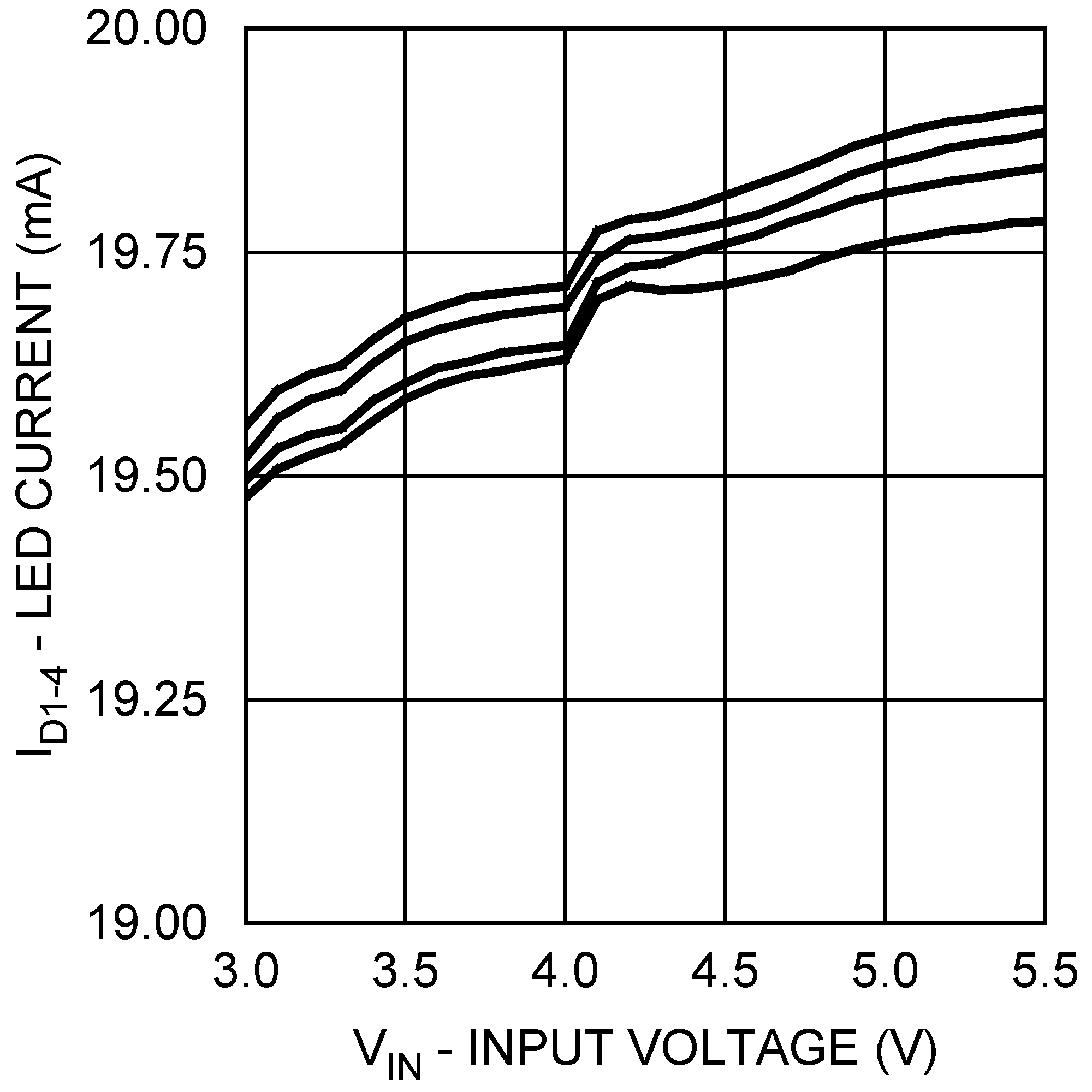
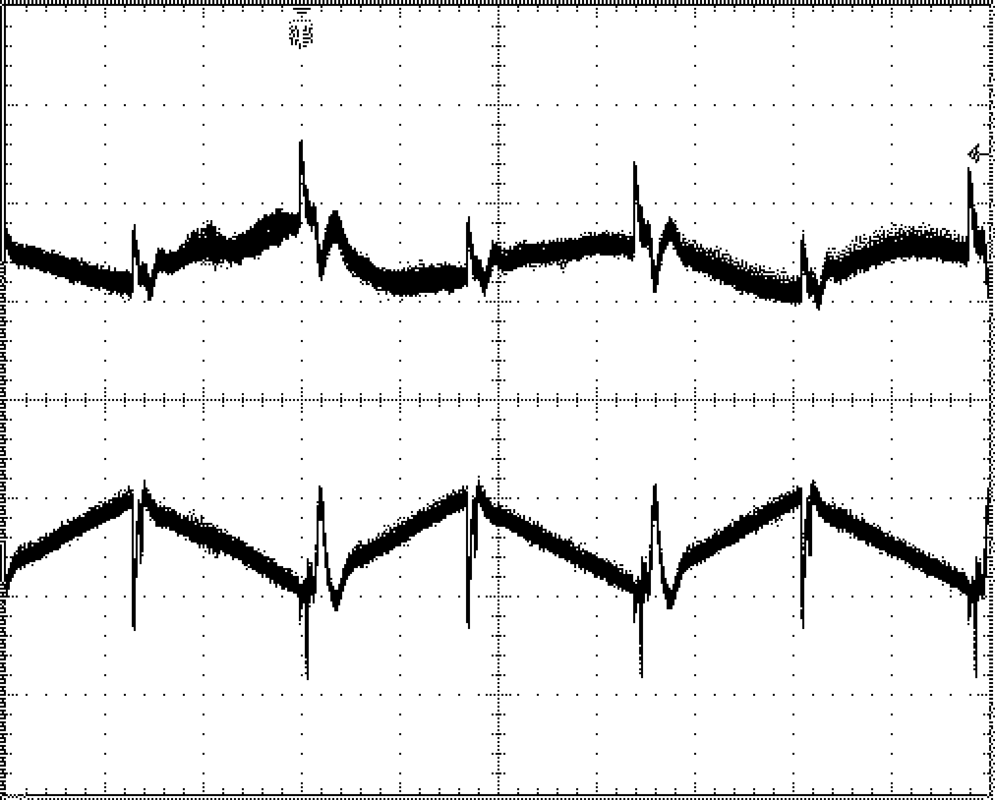
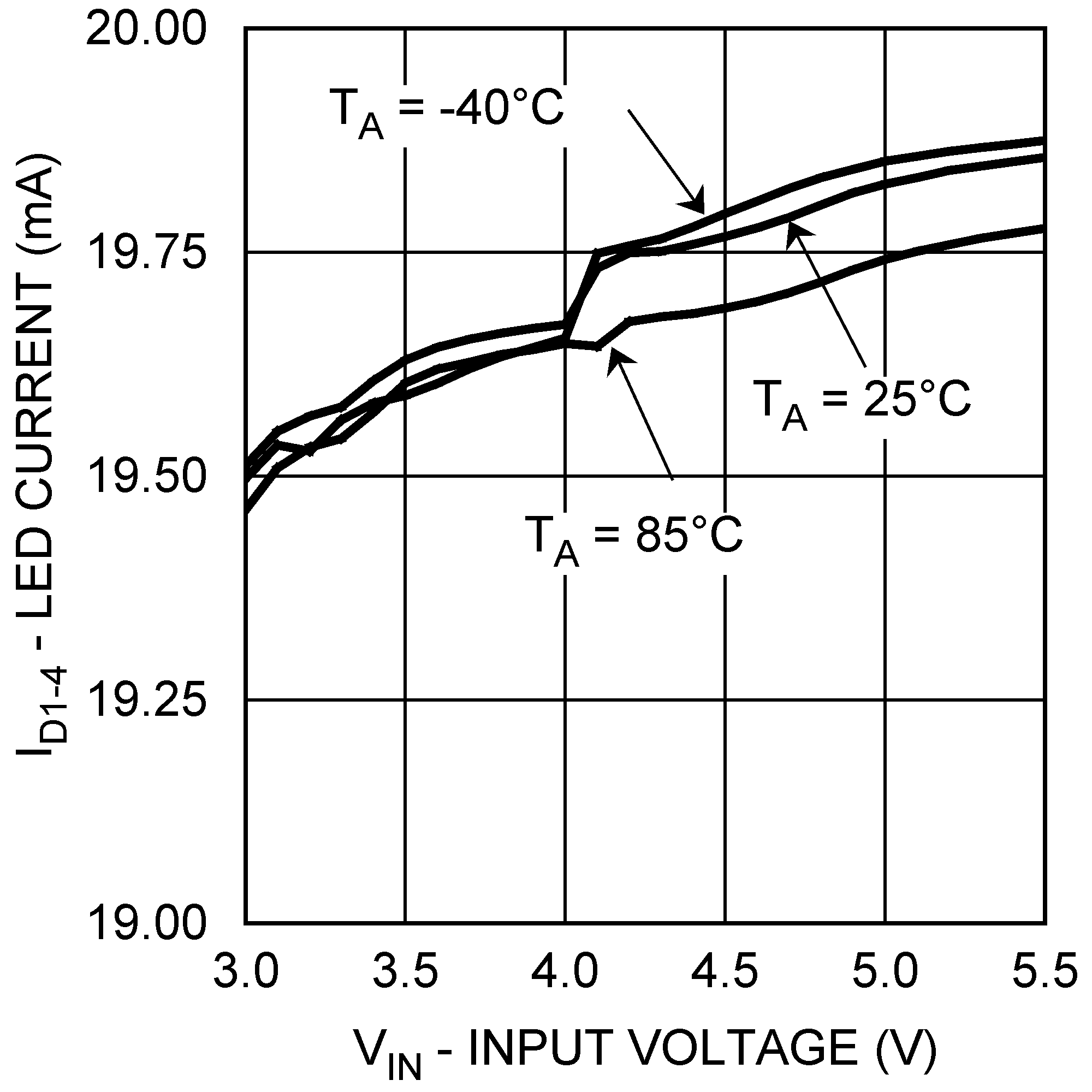
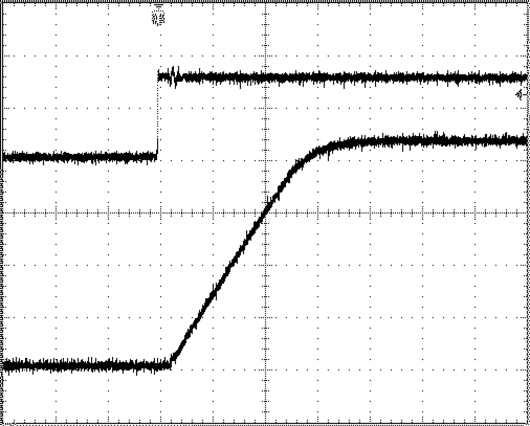
Unless otherwise specified: TA = 25°C, 4 LEDs, VDX = 3.6 V, VIN = 3.6 V, VEN = VIN, VPWM = VIN, C1 = C2 = 1µF, CIN = COUT = 3.3 µF. Capacitors are low-ESR multi-layer ceramic capacitors (MLCCs).

| VIN = 3.6V | Time scale: 400 ns/Div | Load = 15 mA/LED, 4 LEDs |
| CH1 (TOP): VIN; Scale: 20mV/Div, AC Coupled | ||
| CH2 (BOTTOM): VOUT; Scale: 20mV/Div, AC Coupled | ||


| VIN = 3.6 V | Time scale: 100 µs/Div | Load = 20mA/LED, 4 LEDs |
| CH1 (TOP): VEN; Scale: 1 V/Div | ||
| CH2 (BOTTOM): VOUT; Scale: 1 V/Div | ||