SNVS454E August 2006 – December 2014 LM2830 , LM2830-Q1
PRODUCTION DATA.
- 1 Features
- 2 Applications
- 3 Description
- 4 Revision History
- 5 Pin Configuration and Functions
- 6 Specifications
- 7 Detailed Description
-
8 Application and Implementation
- 8.1 Application Information
- 8.2
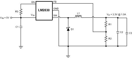
Typical Applications
- 8.2.1 LM2830X Design Vo = 1.2 V at 1.0A
- 8.2.2 LM2830X Design Vo = 0.6 V at 1.0-A
- 8.2.3 LM2830X Design Vo = 3.3 V at 1.0-A
- 8.2.4 LM2830Z Design Vo = 3.3 V at 1.0-A
- 8.2.5 LM2830Z Design Vo = 1.2 V at 1.0-A
- 8.2.6 LM2830X Dual Converters With Delayed Enabled Design
- 8.2.7 LM2830X Buck Converter and Voltage Double Circuit With LDO Follower
- 9 Power Supply Recommendations
- 10Layout
- 11Device and Documentation Support
- 12Mechanical, Packaging, and Orderable Information
Package Options
Mechanical Data (Package|Pins)
- DBV|5
Thermal pad, mechanical data (Package|Pins)
Orderable Information
1 Features
- LM2830Z-Q1 and LM2830X-Q1 in the SOT-23 Package are Automotive-Grade Products that are AEC-Q100 Grade 1 Qualified (–40°C to +125°C Operating Junction Temperature)
- Space-Saving SOT-23 Package
- Input Voltage Range of 3.0 V to 5.5 V
- Output Voltage Range of 0.6 V to 4.5 V
- 1.0-A Output Current
- High Switching Frequencies
- 1.6 MHz (LM2830X)
- 3.0 MHz (LM2830Z)
- 130-mΩ PMOS Switch
- 0.6-V, 2% Internal Voltage Reference
- Internal Soft-Start
- Current Mode, PWM Operation
- Thermal Shutdown
- Overvoltage Protection
2 Applications
- Local 5-V to Vcore Step-Down Converters
- Core Power in HDDs
- Set-Top Boxes
- USB Powered Devices
- DSL Modems
- Automotive
3 Description
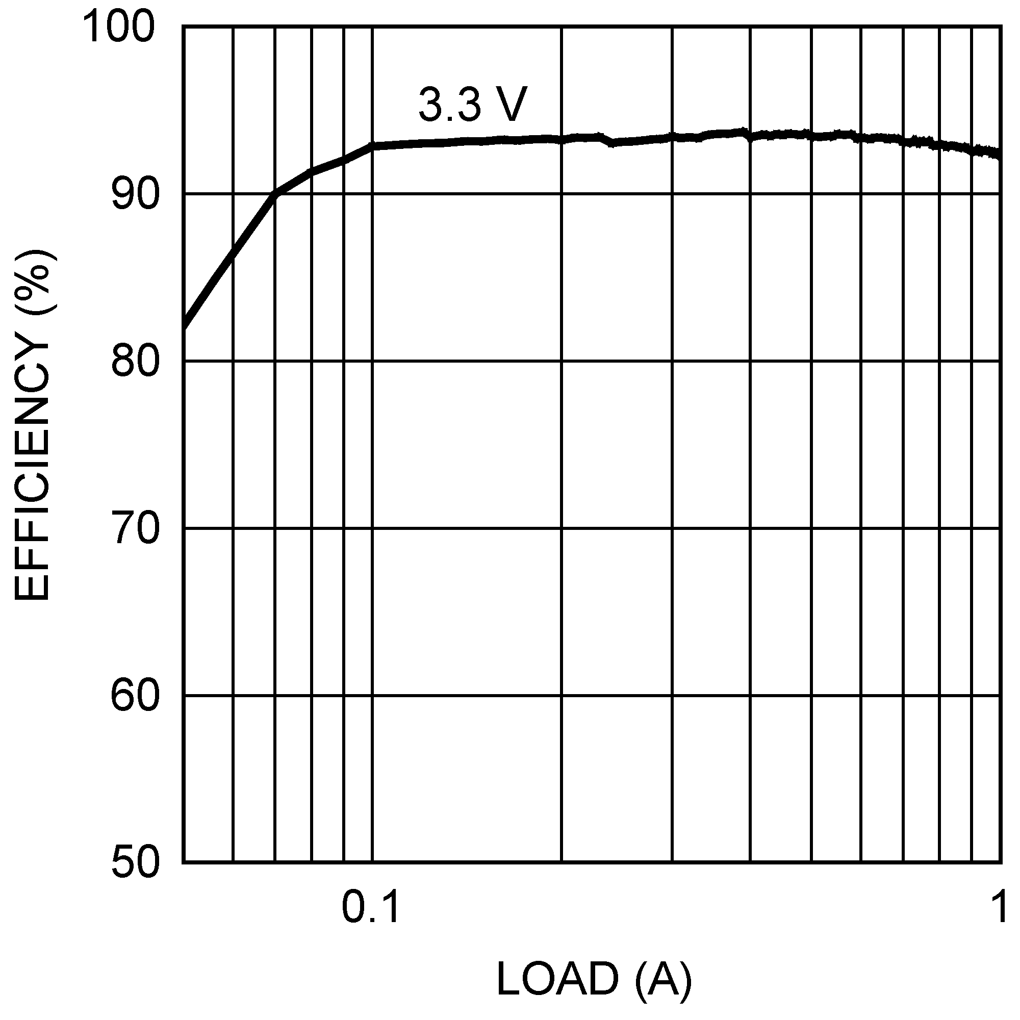
The LM2830 regulator is a monolithic, high-frequency, PWM step-down DC-DC converter in a 5-pin SOT-23 and a 6-Pin WSON package. The device provides all the active functions to provide local DC-DC conversion with fast transient response and accurate regulation in the smallest possible PCB area. With a minimum of external components, the LM2830 regulator is easy to use. The ability to drive 1.0-A loads with an internal 130-mΩ PMOS switch using state-of-the-art 0.5-µm BiCMOS technology results in the best power density available. The world-class control circuitry allows on-times as low as 30 ns, thus supporting exceptionally high frequency conversion over the entire 3-V to 5.5-V input operating range down to the minimum output voltage of 0.6 V. Switching frequency is internally set to 1.6 MHz, or 3.0 MHz, allowing the use of extremely small surface-mount inductors and chip capacitors. Even though the operating frequency is high, efficiencies up to 93% are easy to achieve. External shutdown is included, featuring an ultra-low standby current of 30 nA. The LM2830 regulator uses current-mode control and internal compensation to provide high-performance regulation over a wide range of operating conditions. Additional features include internal soft-start circuitry to reduce inrush current, pulse-by-pulse current limit, thermal shutdown, and output overvoltage protection.
Device Information(1)
| PART NUMBER | PACKAGE | BODY SIZE (NOM) |
|---|---|---|
| LM2830 | SOT (5) | 2.90 mm × 1.60 mm |
| WSON (6) | 3.00 mm × 3.00 mm | |
| LM2830-Q1 | SOT (5) | 2.90 mm × 1.60 mm |
- For all available packages, see the orderable addendum at the end of the datasheet.
Typical Application Circuit
Efficiency vs Load Current