SNVS454E August 2006 – December 2014 LM2830 , LM2830-Q1
PRODUCTION DATA.
- 1 Features
- 2 Applications
- 3 Description
- 4 Revision History
- 5 Pin Configuration and Functions
- 6 Specifications
- 7 Detailed Description
-
8 Application and Implementation
- 8.1 Application Information
- 8.2
Typical Applications
- 8.2.1 LM2830X Design Vo = 1.2 V at 1.0A
- 8.2.2 LM2830X Design Vo = 0.6 V at 1.0-A
- 8.2.3 LM2830X Design Vo = 3.3 V at 1.0-A
- 8.2.4 LM2830Z Design Vo = 3.3 V at 1.0-A
- 8.2.5 LM2830Z Design Vo = 1.2 V at 1.0-A
- 8.2.6 LM2830X Dual Converters With Delayed Enabled Design
- 8.2.7 LM2830X Buck Converter and Voltage Double Circuit With LDO Follower
- 9 Power Supply Recommendations
- 10Layout
- 11Device and Documentation Support
- 12Mechanical, Packaging, and Orderable Information
Package Options
Mechanical Data (Package|Pins)
- DBV|5
Thermal pad, mechanical data (Package|Pins)
Orderable Information
7 Detailed Description
7.1 Overview
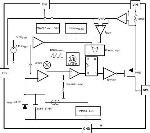
The LM2830 device is a constant frequency PWM buck regulator IC that delivers a 1.0-A load current. The regulator has a preset switching frequency of 1.6 MHz or 3.0 MHz. This high frequency allows the LM2830 device to operate with small surface-mount capacitors and inductors, resulting in a DC-DC converter that requires a minimum amount of board space. The LM2830 device is internally compensated, so it is simple to use and requires few external components. The LM2830 device uses current-mode control to regulate the output voltage.
The following operating description of the LM2830 device will refer to the Simplified Block Diagram (Functional Block Diagram) and to the waveforms in Figure 18. The LM2830 device supplies a regulated output voltage by switching the internal PMOS control switch at constant frequency and variable duty cycle. A switching cycle begins at the falling edge of the reset pulse generated by the internal oscillator. When this pulse goes low, the output control logic turns on the internal PMOS control switch. During this on-time, the SW pin voltage (VSW) swings up to approximately VIN, and the inductor current (IL) increases with a linear slope. IL is measured by the current sense amplifier, which generates an output proportional to the switch current. The sense signal is summed with the regulator’s corrective ramp and compared to the error amplifier’s output, which is proportional to the difference between the feedback voltage and VREF. When the PWM comparator output goes high, the output switch turns off until the next switching cycle begins. During the switch off-time, inductor current discharges through the Schottky catch diode, which forces the SW pin to swing below ground by the forward voltage (VD) of the Schottky catch diode. The regulator loop adjusts the duty cycle (D) to maintain a constant output voltage.
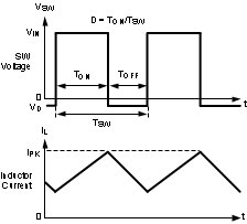 Figure 18. Typical Waveforms
7.2 Functional Block Diagram
7.3 Feature Description
7.3.1 Soft-Start
This function forces VOUT to increase at a controlled rate during start up. During soft-start, the error reference voltage of the amplifier ramps from 0 V to its nominal value of 0.6 V in approximately 600 µs. This forces the regulator output to ramp up in a controlled fashion, which helps reduce inrush current.
7.3.2 Output Overvoltage Protection
The overvoltage comparator compares the FB pin voltage to a voltage that is 15% higher than the internal reference VREF. Once the FB pin voltage goes 15% above the internal reference, the internal PMOS control switch is turned off, which allows the output voltage to decrease toward regulation.
7.3.3 Undervoltage Lockout
Undervoltage lockout (UVLO) prevents the LM2830 device from operating until the input voltage exceeds 2.73 V (typical). The UVLO threshold has approximately 430 mV of hysteresis, so the part will operate until VIN drops below 2.3V (typical). Hysteresis prevents the part from turning off during power up if VIN is nonmonotonic.
7.3.4 Current Limit
The LM2830 device uses cycle-by-cycle current limiting to protect the output switch. During each switching cycle, a current limit comparator detects if the output switch current exceeds 1.75 A (typical), and turns off the switch until the next switching cycle begins.
7.3.5 Thermal Shutdown
Thermal shutdown limits total power dissipation by turning off the output switch when the IC junction temperature exceeds 165°C. After thermal shutdown occurs, the output switch does not turn on until the junction temperature drops to approximately 150°C.
7.4 Device Functional Modes
In normal operational mode, the device will regulate output voltage to the value set with resistive divider.
In addition, this device has an enable (EN) pin that lets the user turn the device on and off by driving this pin high and low. Default setup is that this pin is connected to VIN through pull up resistor (typically 100 kΩ). When enable pin is low the device is in shutdown mode consuming typically only 30 nA, making it ideal for applications where low power consumption is desirable.