SNVS454E August 2006 – December 2014 LM2830 , LM2830-Q1
PRODUCTION DATA.
- 1 Features
- 2 Applications
- 3 Description
- 4 Revision History
- 5 Pin Configuration and Functions
- 6 Specifications
- 7 Detailed Description
-
8 Application and Implementation
- 8.1 Application Information
- 8.2
Typical Applications
- 8.2.1 LM2830X Design Vo = 1.2 V at 1.0A
- 8.2.2 LM2830X Design Vo = 0.6 V at 1.0-A
- 8.2.3 LM2830X Design Vo = 3.3 V at 1.0-A
- 8.2.4 LM2830Z Design Vo = 3.3 V at 1.0-A
- 8.2.5 LM2830Z Design Vo = 1.2 V at 1.0-A
- 8.2.6 LM2830X Dual Converters With Delayed Enabled Design
- 8.2.7 LM2830X Buck Converter and Voltage Double Circuit With LDO Follower
- 9 Power Supply Recommendations
- 10Layout
- 11Device and Documentation Support
- 12Mechanical, Packaging, and Orderable Information
Package Options
Mechanical Data (Package|Pins)
- DBV|5
Thermal pad, mechanical data (Package|Pins)
Orderable Information
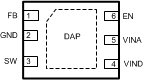
5 Pin Configuration and Functions
WSON Package
6-Pin
Top View
SOT Package
5-Pins
Top View
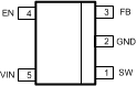
Pin Functions (5-Pin SOT)
| PIN | I/O(1) | DESCRIPTION | |
|---|---|---|---|
| NAME | NO. | ||
| SW | 1 | O | Output switch. Connect to the inductor and catch diode. |
| GND | 2 | G | Signal and power ground pin. Place the bottom resistor of the feedback network as close as possible to this pin. |
| FB | 3 | I | Feedback pin. Connect to external resistor divider to set output voltage. |
| EN | 4 | I | Enable control input. Logic high enables operation. Do not allow this pin to float or be greater than VIN + 0.3 V. |
| VIN | 5 | I/P | Input supply voltage. |
(1) I: Input Pin, O: Output Pin, P: Power Pin, G: Ground Pin
Pin Functions (6-Pin WSON)
| PIN | I/O(1) | DESCRIPTION | |
|---|---|---|---|
| NAME | NO. | ||
| FB | 1 | I | Feedback pin. Connect to external resistor divider to set output voltage. |
| GND | 2 | G | Signal and power ground pin. Place the bottom resistor of the feedback network as close as possible to this pin. |
| SW | 3 | O | Output switch. Connect to the inductor and catch diode. |
| VIND | 4 | I/P | Power Input supply. |
| VINA | 5 | I/P | Control circuitry supply voltage. Connect VINA to VIND on PC board. |
| EN | 6 | I | Enable control input. Logic high enables operation. Do not allow this pin to float or be greater than VINA + 0.3V. |
| Die Attach Pad | – | – | Connect to system ground for low thermal impedance, but it cannot be used as a primary GND connection. |
(1) I: Input Pin, O: Output Pin, P: Power Pin, G: Ground Pin