SNVS459A October 2006 – September 2017 LM2853
PRODUCTION DATA.
- 1 Features
- 2 Applications
- 3 Description
- 4 Revision History
- 5 Pin Configuration and Functions
- 6 Specifications
- 7 Detailed Description
-
8 Application and Implementation
- 8.1
Application Information
- 8.1.1 Input Capacitor (CIN)
- 8.1.2 Soft-Start Capacitor (CSS)
- 8.1.3 Soft-Start Capacitor (CSS) and Fault Conditions
- 8.1.4 Compensation
- 8.1.5 Output Filter Values
- 8.1.6 Choosing an Inductance Value
- 8.1.7 Output Filter Inductors
- 8.1.8 Output Filter Capacitors
- 8.1.9 Split-Rail Operation
- 8.1.10 Switch Node Protection
- 8.2 Typical Application
- 8.1
Application Information
- 9 Layout
- 10Device and Documentation Support
- 11Mechanical, Packaging, and Orderable Information
Package Options
Mechanical Data (Package|Pins)
- PWP|14
Thermal pad, mechanical data (Package|Pins)
- PWP|14
Orderable Information
6 Specifications
6.1 Absolute Maximum Ratings
over operating free-air temperature range (unless otherwise noted)(1)| MIN | MAX | UNIT | ||
|---|---|---|---|---|
| AVIN, PVIN, EN, SNS, SW, SS | –0.3 | 6 | V | |
| Power Dissipation | Internally Limited | V | ||
| 14-Pin Exposed Pad HTSSOP Package (PWP) | Infrared (15 sec) | 220 | °C | |
| Vapor Phase (60 sec) | 215 | °C | ||
| Soldering (10 sec) | 260 | °C | ||
| Maximum junction temperature | 150 | °C | ||
| Storage temperature, Tstg | –65 | 150 | °C | |
(1) Stresses beyond those listed under Absolute Maximum Ratings may cause permanent damage to the device. These are stress ratings only, which do not imply functional operation of the device at these or any other conditions beyond those indicated under Recommended Operating Conditions. Exposure to absolute-maximum-rated conditions for extended periods may affect device reliability.
6.2 ESD Ratings
| VALUE | UNIT | |||
|---|---|---|---|---|
| V(ESD) | Electrostatic discharge | Human-body model (HBM), per ANSI/ESDA/JEDEC JS-001(1) | ±2 | kV |
(1) JEDEC document JEP155 states that 500-V HBM allows safe manufacturing with a standard ESD control process.
6.3 Recommended Operating Conditions
over operating free-air temperature range (unless otherwise noted) (1)| MIN | MAX | UNIT | ||
|---|---|---|---|---|
| PVIN to GND | 1.5 | 5.5 | V | |
| AVIN to GND | 3 | 5.5 | V | |
| Operation junction temperature, TJ | –40 | 125 | °C | |
6.4 Thermal Information
| THERMAL METRIC(1) | LM2853 | UNIT | |
|---|---|---|---|
| PWP (HTSSOP) | |||
| 14 PINS | |||
| RθJA | Junction-to-ambient thermal resistance | 38 | °C/W |
(1) For more information about traditional and new thermal metrics, see the Semiconductor and IC Package Thermal Metrics application report.
6.5 Electrical Characteristics
Specifications with standard typeface are for TJ = 25°C. Minimum and Maximum limits are ensured through test, design or statistical correlation. Typical values represent the most likely parametric norm at TJ = 25°C and are provided for reference purposes only. Unless otherwise specified AVIN = PVIN = 5 V.| PARAMETER | TEST CONDITIONS | MIN | TYP | MAX | UNIT | ||
|---|---|---|---|---|---|---|---|
| SYSTEM PARAMETERS | |||||||
| VOUT | Voltage tolerance (2) | VOUT = 0.8 V option | TJ = –40°C to 125°C | 0.782 | 0.8 | 0.818 | V |
| VOUT = 1 V option | TJ = –40°C to 125°C | 0.9775 | 1 | 1.0225 | |||
| VOUT = 1.2 V option | TJ = –40°C to 125°C | 1.1730 | 1.2 | 1.227 | |||
| VOUT = 1.5 V option | TJ = –40°C to 125°C | 1.4663 | 1.5 | 1.5337 | |||
| VOUT = 1.8 V option | TJ = –40°C to 125°C | 1.7595 | 1.8 | 1.8405 | |||
| VOUT = 2.5 V option | TJ = –40°C to 125°C | 2.4437 | 2.5 | 2.5563 | |||
| VOUT = 3 V option | TJ = –40°C to 125°C | 2.9325 | 3 | 3.0675 | |||
| VOUT = 3.3 V option | TJ = –40°C to 125°C | 3.2257 | 3.3 | 3.3743 | |||
| ΔVOUT/ΔAVIN | Line regulation (2) | VOUT = 0.8 V, 1 V, 1.2 V, 1.5 V, 1.8 V or 2.5 V 3 V ≤ AVIN ≤ 5.5 V |
TJ = –40°C to 125°C | 0.2 | 1.1 | % | |
| VOUT = 3 V or 3.3 V 3.5 V ≤ AVIN ≤ 5.5 V |
TJ = –40°C to 125°C | 0.2 | 1.1 | % | |||
| ΔVOUT/ΔIO | Load regulation | Normal operation | 2 | mV/A | |||
| VON | UVLO Threshold (AVIN) | Rising | TJ = –40°C to 125°C | 2.47 | 3 | V | |
| Falling hysteresis | TJ = –40°C to 125°C | 50 | 155 | 260 | mV | ||
| RDS(ON)-P | PFET On resistance | Isw = 3A | TJ = –40°C to 125°C | 40 | 120 | mΩ | |
| RDS(ON)-N | NFET On resistance | Isw = 3A | TJ = –40°C to 125°C | 32 | 100 | mΩ | |
| RSS | Soft-Start resistance | 450 | kΩ | ||||
| ICL | Peak current limit threshold | 3.6 | 5 | A | |||
| IQ | Operating current | Non-switching | TJ = –40°C to 125°C | 0.85 | 2 | mA | |
| ISD | Shutdown quiescent current | EN = 0 V | TJ = –40°C to 125°C | 12 | 50 | µA | |
| RSNS | Sense pin resistance | 432 | kΩ | ||||
| PWM | |||||||
| fosc | Switching frequency | . | TJ = –40°C to 125°C | 325 | 550 | 725 | kHz |
| Drange | Duty cycle range | TJ = –40°C to 125°C | 0 | 100 | % | ||
| ENABLE CONTROL (3) | |||||||
| VIH | EN Pin minimum high input | TJ = –40°C to 125°C | 75 | % of AVIN | |||
| VIL | EN Pin maximum low input | TJ = –40°C to 125°C | 25 | % of AVIN | |||
| IEN | EN Pin pullup current | EN = 0 V | 1.5 | µA | |||
| THERMAL CONTROLS | |||||||
| TSD | Thermal shutdown threshold | 165 | °C | ||||
| TSD-HYS | Hysteresis for thermal shutdown | 10 | °C | ||||
(1) Absolute maximum ratings indicate limits beyond which damage to the device may occur. Operating Range indicates conditions for which the device is intended to be functional, but does not ensure specific performance limits. For ensured specifications and test conditions, see the Electrical Characteristics.
(2) VOUT measured in a non-switching, closed-loop configuration at the SNS pin.
(3) The enable pin is internally pulled up, so the LM2853 is automatically enabled unless an external enable voltage is applied.
6.6 Typical Characteristics
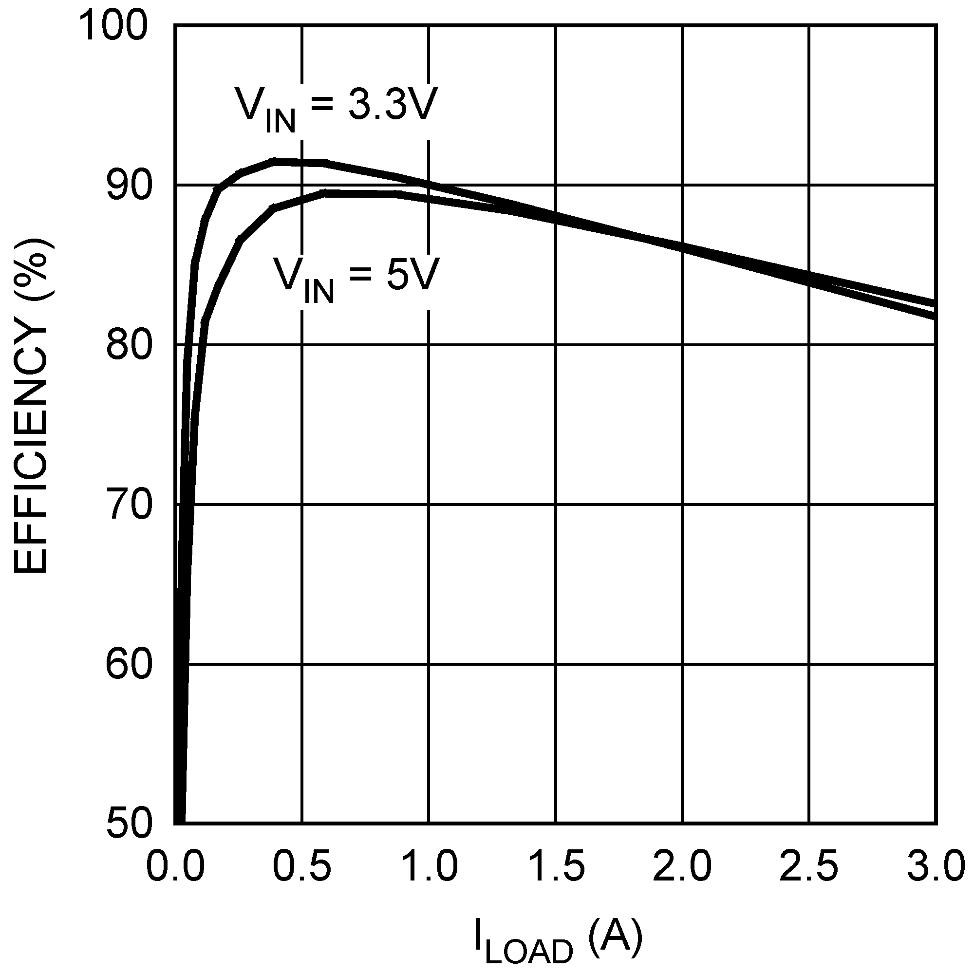
| VOUT = 1.8 V | ||
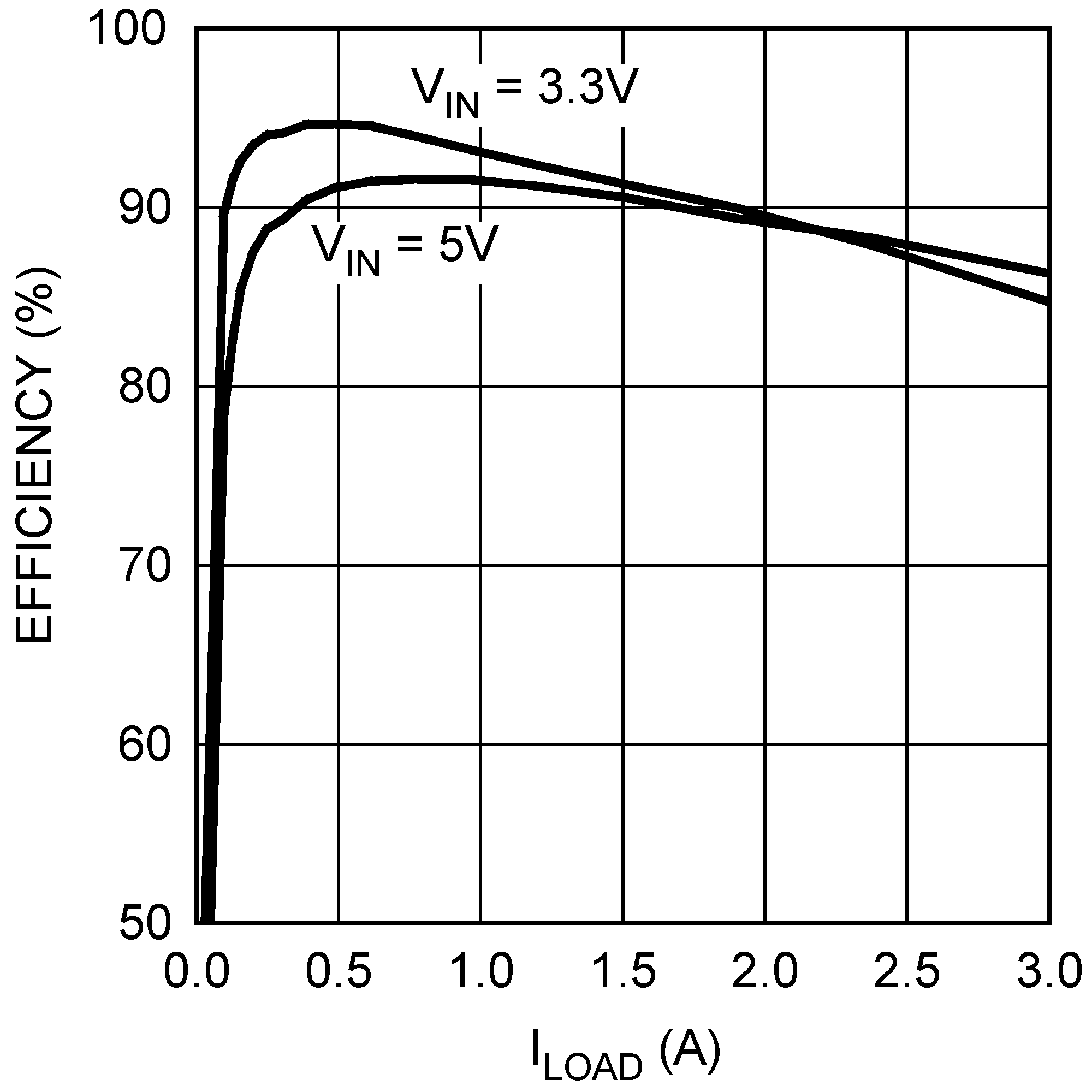
| VOUT = 2.5 V | ||
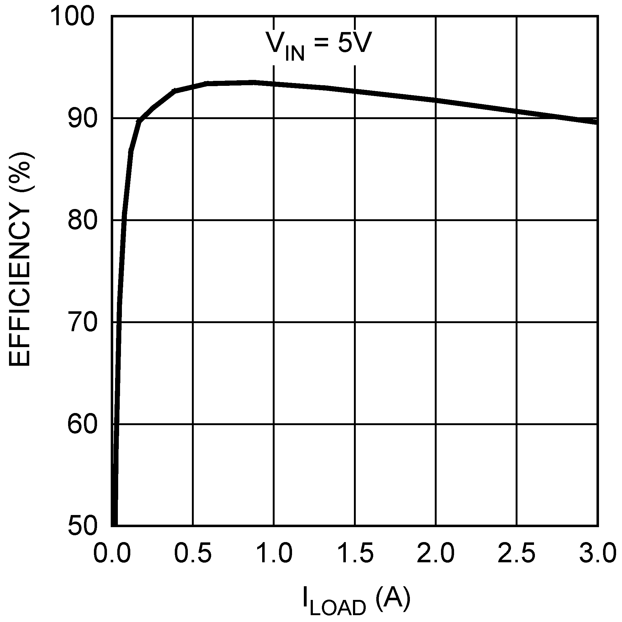
| VOUT = 3.3 V | ||
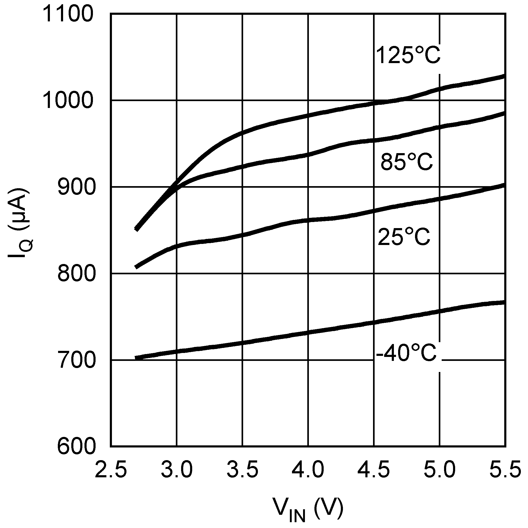 Figure 7. IQ vs VIN and Temperature
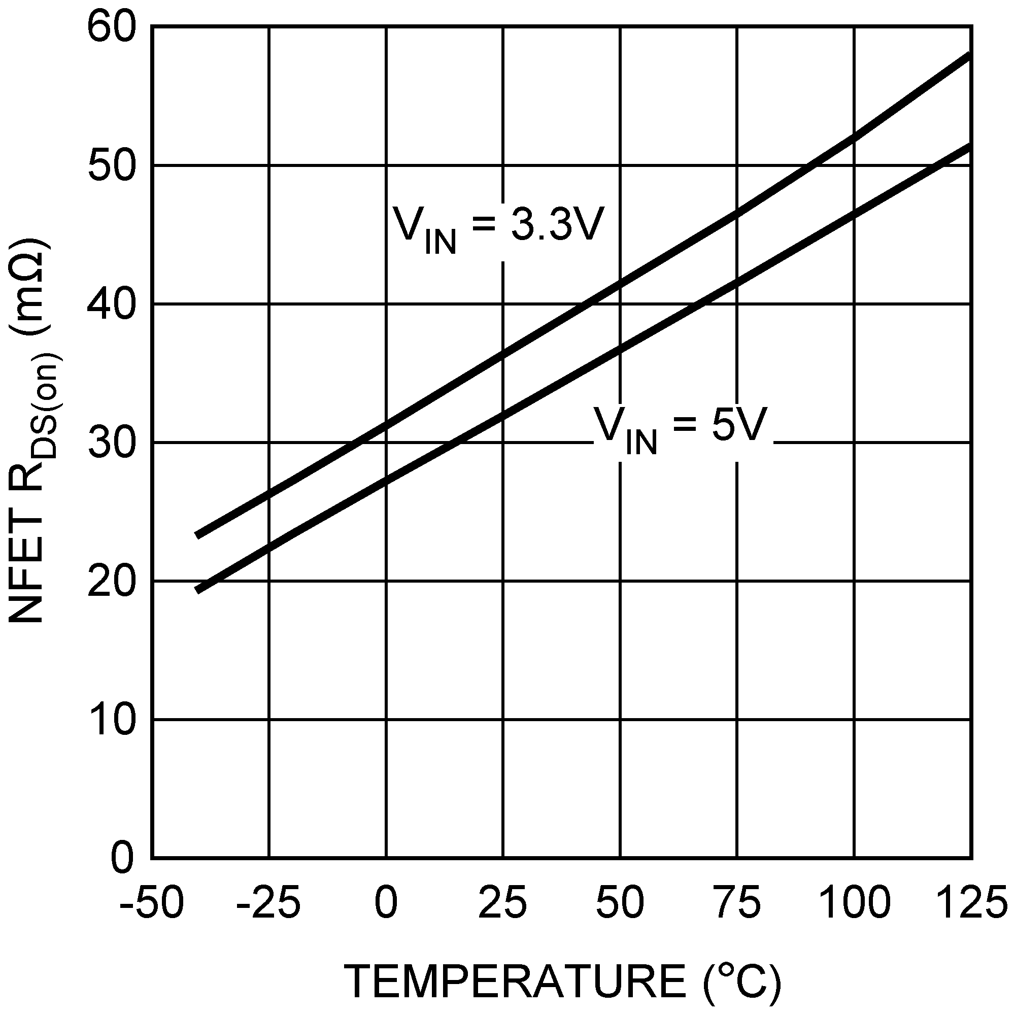
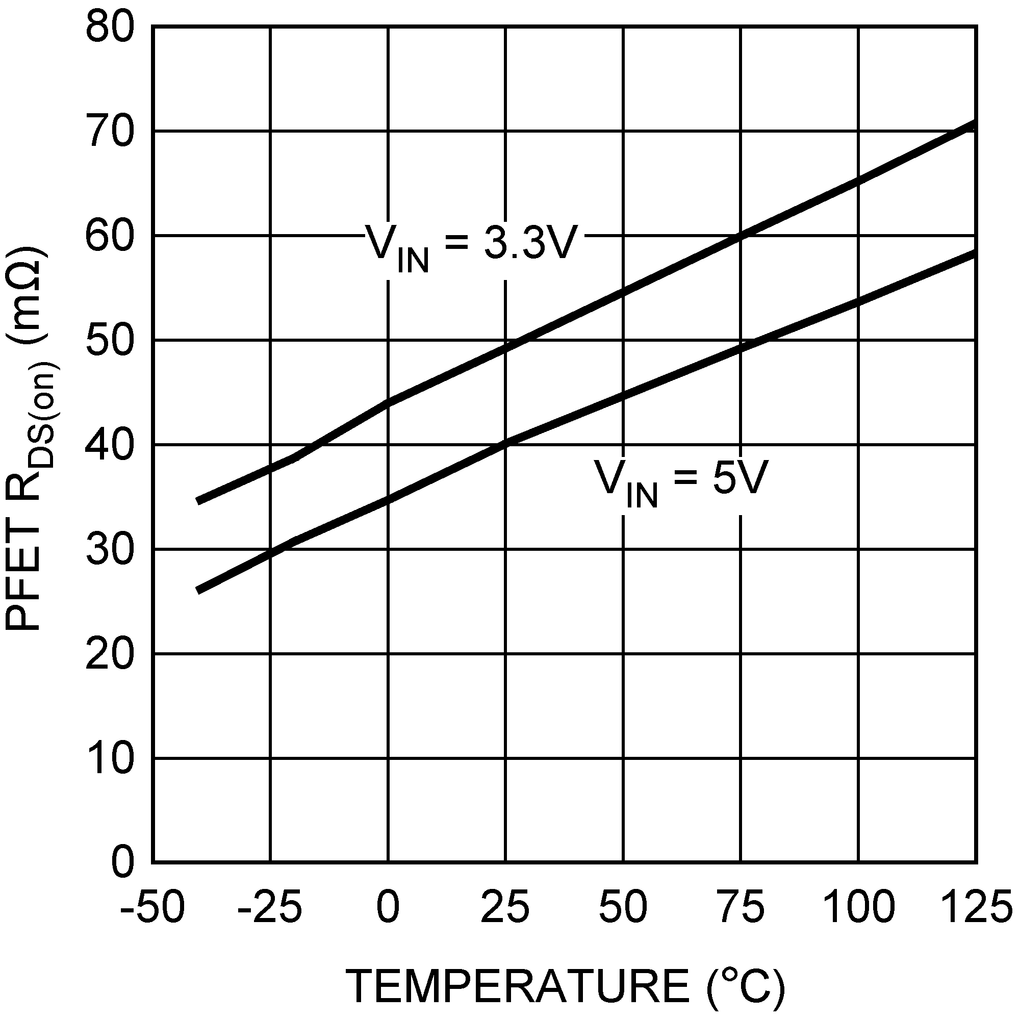
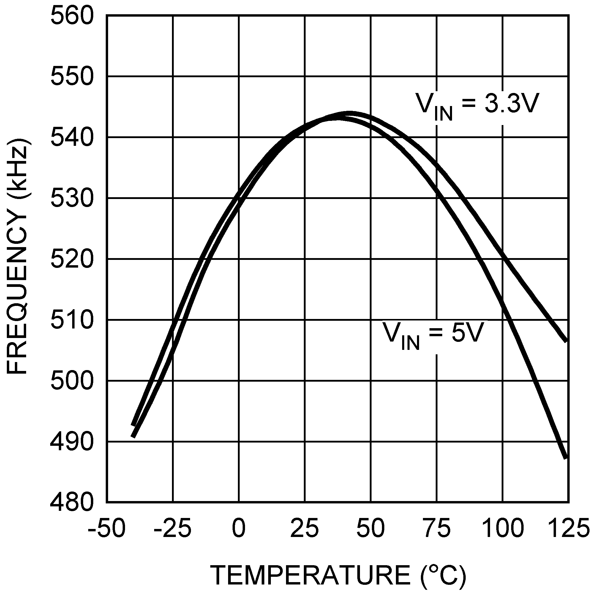
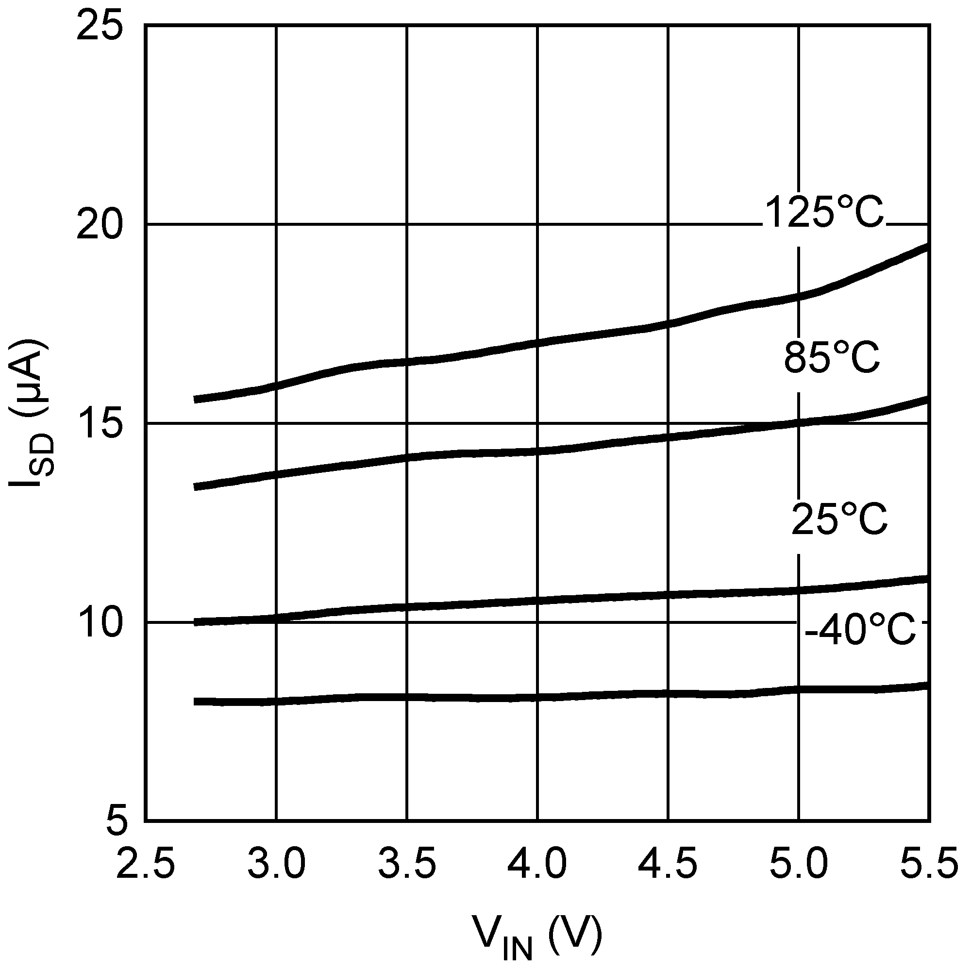 Figure 8. ISD vs VIN and Temperature