SNVS560E March 2008 – October 2017 LM2854
PRODUCTION DATA.
- 1 Features
- 2 Applications
- 3 Description
- 4 Revision History
- 5 Pin Configuration and Functions
- 6 Specifications
- 7 Detailed Description
-
8 Application and Implementation
- 8.1 Application Information
- 8.2
Typical Application
- 8.2.1 Design Requirements
- 8.2.2
Detailed Design Procedure
- 8.2.2.1 Input Filter Capacitor
- 8.2.2.2 AVIN Filtering Components
- 8.2.2.3 Soft-Start Capacitor
- 8.2.2.4 Tracking - Equal Soft-Start Time
- 8.2.2.5 Tracking - Equal Slew Rates
- 8.2.2.6 Enable and UVLO
- 8.2.2.7 Output Voltage Setting
- 8.2.2.8 Compensation Component Selection
- 8.2.2.9 Filter Inductor and Output Capacitor Selection
- 8.2.3 Application Curves
- 8.2.4 System Examples
- 9 Power Supply Recommendations
- 10Layout
- 11Device and Documentation Support
- 12Mechanical, Packaging, and Orderable Information
Package Options
Mechanical Data (Package|Pins)
- PWP|16
Thermal pad, mechanical data (Package|Pins)
- PWP|16
Orderable Information
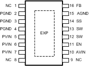
5 Pin Configuration and Functions
PWP Package
16-Pin HTSSOP
Top View

Pin Functions
| PIN | I/O | DESCRIPTION | |
|---|---|---|---|
| NAME | NO. | ||
| NC | 1, 8, 9 | — | Reserved for factory use, this pin should be connected to GND to ensure proper operation. |
| PGND | 2, 3, 4 | — | Power ground pins for the internal power switches. These pins should be connected together locally at the device and tied to the PC board ground plane. |
| PVIN | 5, 6, 7 | — | Input voltage to the power switches inside the device. These pins should be connected together at the device. A low ESR input capacitance should be located as close as possible to these pins. |
| AVIN | 10 | — | Analog input voltage supply that generates the internal bias. The UVLO circuit derives its input from this pin also. Thus, if the voltage on AVIN falls below the UVLO threshold, both internal FETs are turned off. TI recommends connecting PVIN to AVIN through a low pass RC filter to minimize the influence of input rail ripple and noise on the analog control circuitry. The series resistor should be 1 Ω and the bypass capacitor should be a X7R ceramic type 0.1 µF to 1 µF. |
| EN | 11 | I | Active high enable input for the device. Typically, turnon threshold is 1.23 V with 0.15-V hysteresis. An external resistor divider from PVIN can be used to effectively increase the UVLO turnon threshold. If not used, the EN pin should be connected to PVIN. |
| SW | 12, 13 | O | Switch node pins. This is the PWM output of the internal MOSFET power switches. These pins should be tied together locally and connected to the filter inductor. |
| SS | 14 | I/O | Soft-start control pin. An internal 2-µA current source charges an external capacitor connected between this pin and AGND to set the output voltage ramp rate during start-up. This pin can also be used to configure the tracking feature. |
| AGND | 15 | — | Quiet analog ground for the internal bias circuitry. |
| FB | 16 | I | Feedback pin is connected to the inverting input of the voltage loop error amplifier. An 0.8-V bandgap reference is connected to the noninverting input of the error amplifier. |
| Exposed Pad | — | Exposed metal pad on the underside of the package with a weak electrical connection to PGND. TI recommends connecting this pad to the PC board ground plane in order to improve thermal dissipation. | |