SLCS142H December 2003 – May 2025 LM2901-Q1 , LM2901AV-Q1 , LM2901B-Q1 , LM2901V-Q1
PRODUCTION DATA
- 1
- 1 Features
- 2 Applications
- 3 Description
- 4 Pin Configuration and Functions
-
5 Specifications
- 5.1 Absolute Maximum Ratings for LM2901B-Q1
- 5.2 Absolute Maximum Ratings for LM2901x-Q1
- 5.3 ESD Ratings
- 5.4 Recommended Operating Conditions for LM2901B-Q1
- 5.5 Recommended Operating Conditions for LM2901x-Q1
- 5.6 Thermal Information
- 5.7 Electrical Characteristics for LM2901B-Q1
- 5.8 Switching Characteristics for LM2901B-Q1
- 5.9 Electrical Characteristics for LM2901x-Q1
- 5.10 Switching Characteristics for LM2901x-Q1
- 5.11 Typical Characteristics
- 6 Detailed Description
- 7 Application and Implementation
- 8 Device and Documentation Support
- 9 Revision History
- 10Mechanical, Packaging, and Orderable Information
Package Options
Refer to the PDF data sheet for device specific package drawings
Mechanical Data (Package|Pins)
- D|14
- PW|14
Thermal pad, mechanical data (Package|Pins)
Orderable Information
4 Pin Configuration and Functions
 Figure 4-1 D, PW and DYY Packages
14-Pin SOIC, TSSOP and SOT-23
Top View
 Figure 4-3 RUC Package
14-Pad X2QFN
Top View

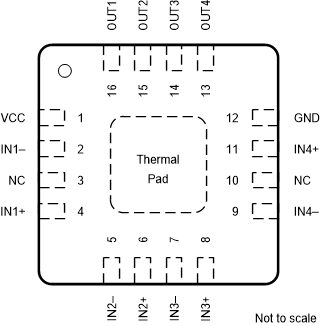
NOTE: Connect
exposed thermal pad directly to GND pin.
Figure 4-2 RTE Package16-Pad WQFN With Exposed Thermal Pad
Top View
Table 4-1 Pin Functions
| PIN | I/O | DESCRIPTION | |||
|---|---|---|---|---|---|
| NAME(1) | SOIC, TSSOP, DYY |
X2QFN | WQFN | ||
| OUT1 (1) | 1 | 14 | 16 | Output | Output pin of the comparator 2 |
| OUT2 (1) | 2 | 1 | 15 | Output | Output pin of the comparator 1 |
| VCC | 3 | 2 | 1 | — | Positive supply |
| IN2– (1) | 4 | 3 | 5 | Input | Negative input pin of the comparator 1 |
| IN2+ (1) | 5 | 4 | 6 | Input | Positive input pin of the comparator 1 |
| IN1– (1) | 6 | 5 | 2 | Input | Negative input pin of the comparator 2 |
| IN1+ (1) | 7 | 6 | 4 | Input | Positive input pin of the comparator 2 |
| IN3– | 8 | 7 | 7 | Input | Negative input pin of the comparator 3 |
| IN3+ | 9 | 8 | 8 | Input | Positive input pin of the comparator 3 |
| IN4– | 10 | 9 | 9 | Input | Negative input pin of the comparator 4 |
| IN4+ | 11 | 10 | 11 | Input | Positive input pin of the comparator 4 |
| GND | 12 | 11 | 12 | — | Negative supply |
| OUT4 | 13 | 12 | 13 | Output | Output pin of the comparator 4 |
| OUT3 | 14 | 13 | 14 | Output | Output pin of the comparator 3 |
| NC | — | — | 3 | — | No Internal Connection - Leave floating or GND |
| NC | — | — | 10 | — | No Internal Connection - Leave floating or GND |
| Thermal Pad | — | — | PAD | — | Connect directly to GND pin |
(1) Some manufacturers transpose the names of channels 1 & 2. Electrically the pinouts are identical, just a difference in channel naming convention.