SNVS093G June 1999 – May 2015 LM2990
PRODUCTION DATA.
- 1 Features
- 2 Applications
- 3 Description
- 4 Revision History
- 5 Pin Configuration and Functions
- 6 Specifications
- 7 Detailed Description
- 8 Application and Implementation
- 9 Power Supply Recommendations
- 10Layout
- 11Device and Documentation Support
- 12Mechanical, Packaging, and Orderable Information
Package Options
Mechanical Data (Package|Pins)
Thermal pad, mechanical data (Package|Pins)
- KTT|3
Orderable Information
8 Application and Implementation
NOTE
Information in the following applications sections is not part of the TI component specification, and TI does not warrant its accuracy or completeness. TI’s customers are responsible for determining suitability of components for their purposes. Customers should validate and test their design implementation to confirm system functionality.
8.1 Application Information
The LM2990 is a 1-A negative voltage regulator with an operating VIN range of –6 V to –26 V, and a regulated VOUT having 5% accuracy with a maximum rated IOUT current of 1 A. Efficiency is defined by the ratio of output voltage to input voltage because the LM2990 is a linear voltage regulator. To achieve high efficiency, the dropout voltage (VIN – VOUT) must be as small as possible, thus requiring a very low dropout LDO.
Successfully implementing an LDO in an application depends on the application requirements. If the requirements are simply input voltage and output voltage, compliance specifications (such as internal power dissipation or stability) must be verified to ensure a solid design. If timing, start-up, noise, PSRR, or any other transient specification is required, the design becomes more challenging.
8.2 Typical Application
8.2.1 –5 V Post Regulator for an Isolated Switching Power Supply
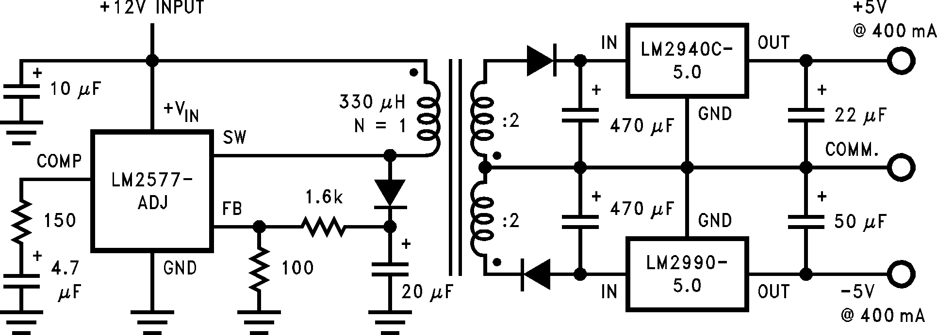 Figure 20. Post Regulator for an Isolated Switching Power Supply
8.2.1.1 Design Requirements
For this design example, use the parameters listed in Table 1 as the input parameters.
8.2.1.2 Detailed Design Procedure
At 400-mA loading, the dropout of the LM2990 has 1-V maximum dropout over temperature, thus an –5 V headroom is sufficient for operation over both input and output voltage accuracy. The efficiency of the LM2990 in this configuration is VOUT / VIN = 50%.
To achieve the smallest form factor, the TO-263(KTT) package is selected. Input and output capacitors should be selected in accordance with the External Capacitors section. Aluminum capacitances of 470 μF for the input and 50-μF capacitors for the output are selected. With an efficiency of 50% and a 400-mA maximum load, the internal power dissipation is 2000 mW, which corresponds to 82.5°C junction temperature rise for the TO-263 package. With an 25°C ambient temperature, the junction temperature is at 107.5°C.
8.2.1.2.1 External Capacitors
The LM2990 regulator requires an output capacitor to maintain stability. The capacitor must be at least 10-μF aluminum electrolytic or 1-μF solid tantalum. The equivalent series resistance (ESR) of the output capacitor must be less than 10 Ω, or the zero added to the regulator frequency response by the ESR could reduce the phase margin, creating oscillations. An input capacitor, of at least 1-μF solid tantalum or 10-μF aluminum electrolytic, is also needed if the regulator is situated more than 6 from the input power supply filter.
8.2.1.2.2 Forcing The Output Positive
Due to an internal clamp circuit, the LM2990 can withstand positive voltages on its output. If the voltage source pulling the output positive is DC, the current must be limited to 1.5 A. A current over 1.5 A fed back into the LM2990 could damage the device. The LM2990 output can also withstand fast positive voltage transients up to 26V, without any current limiting of the source. However, if the transients have a duration of over 1 ms, the output should be clamped with a Schottky diode to ground.
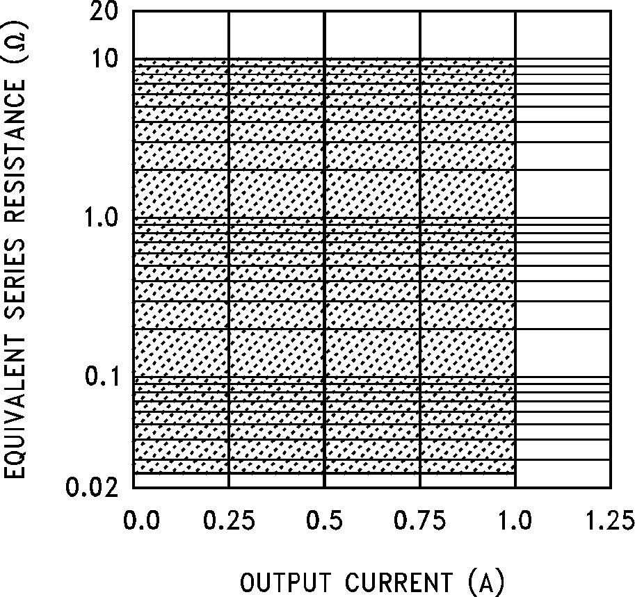 Figure 21. Output Capacitor ESR
8.2.1.3 Application Curves
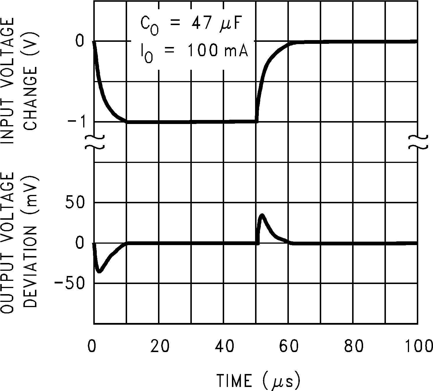 Figure 22. LM2990-5 Line Transient Response
 Figure 23. LM2990-5 Load Transient Response
8.2.2 Fixed or Adjustable Current Sink
The LM2990 is configurable as a fixed or adjustable current sink. As Figure 24 and Figure 25 show, the sink current is determined by the resistor value — to achieve adjustable sink current, add one adjustable resistor between output and load.
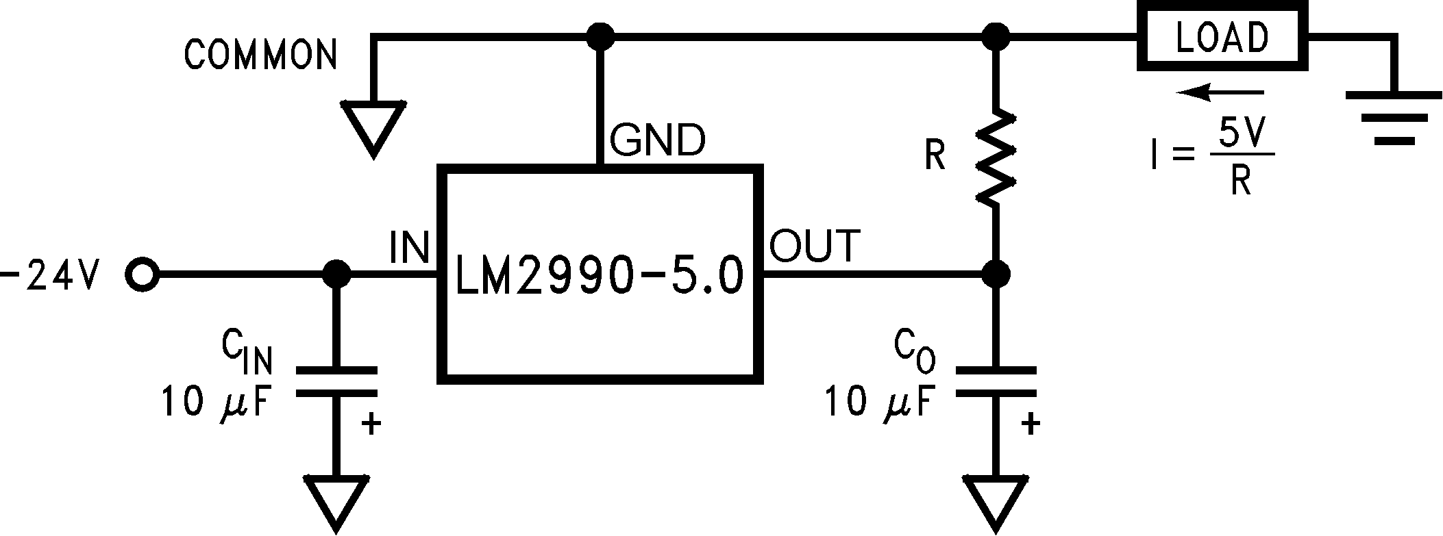 Figure 24. Fixed Current Sink
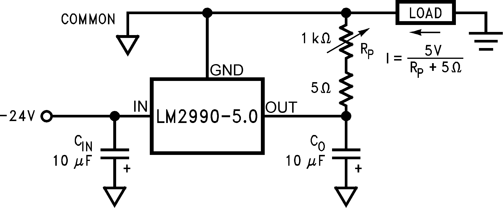 Figure 25. Adjustable Current Sink
8.2.2.1 Design Requirements
See Design Requirements.
8.2.2.2 Detailed Design Procedure
8.2.2.3 Application Curves
See Application Curves.