SNVS093G June 1999 – May 2015 LM2990
PRODUCTION DATA.
- 1 Features
- 2 Applications
- 3 Description
- 4 Revision History
- 5 Pin Configuration and Functions
- 6 Specifications
- 7 Detailed Description
- 8 Application and Implementation
- 9 Power Supply Recommendations
- 10Layout
- 11Device and Documentation Support
- 12Mechanical, Packaging, and Orderable Information
Package Options
Mechanical Data (Package|Pins)
Thermal pad, mechanical data (Package|Pins)
- KTT|3
Orderable Information
6 Specifications
6.1 Absolute Maximum Ratings
over operating free-air temperature range (unless otherwise noted) (1)(2)| MIN | MAX | UNIT | ||
|---|---|---|---|---|
| Input voltage | –26 | 0.3 | V | |
| Power dissipation(3) | Internally limited | |||
| Junction temperature (TJmax) | 125 | °C | ||
| Storage temperature, Tstg | –65 | 150 | °C | |
(1) Stresses beyond those listed under Absolute Maximum Ratings may cause permanent damage to the device. These are stress ratings only, which do not imply functional operation of the device at these or any other conditions beyond those indicated under Recommended Operating Conditions. Exposure to absolute-maximum-rated conditions for extended periods may affect device reliability.
(2) If Military/Aerospace specified devices are required, please contact the Texas Instruments Sales Office/Distributors for availability and specifications.
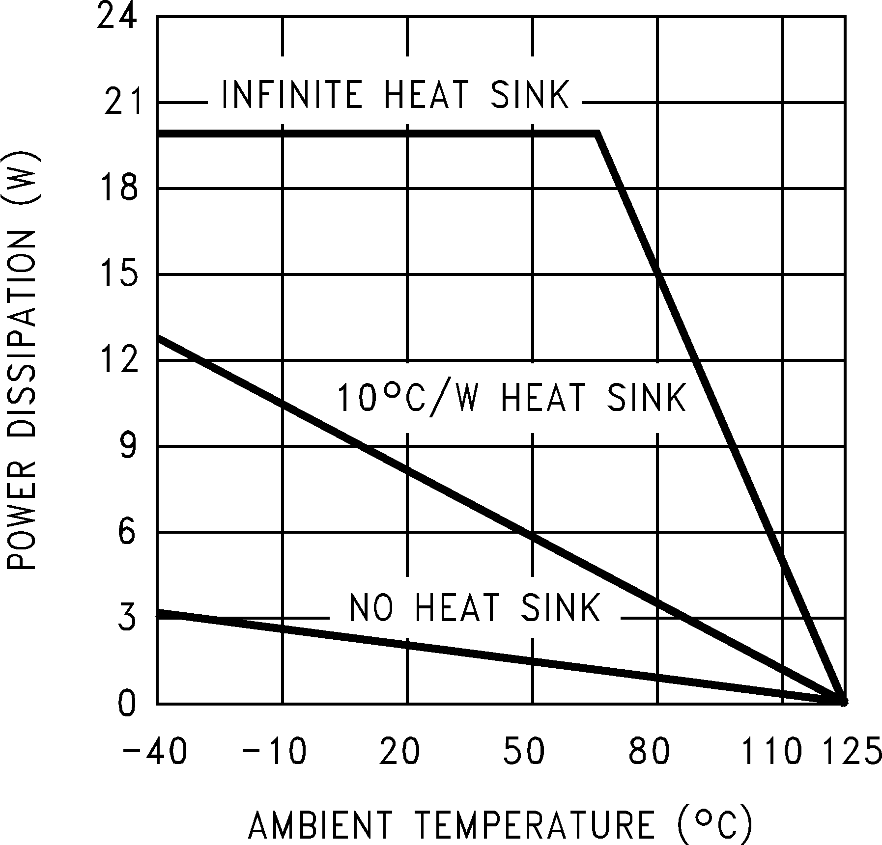
(3) The maximum power dissipation is a function of TJmax, RθJA, and TA. The maximum allowable power dissipation at any ambient temperature is PD = (TJmax − TA)/RθJA. If this dissipation is exceeded, the die temperature will rise above 125°C, and the LM2990 will eventually go into thermal shutdown at a TJ of approximately 160°C. Please refer to Thermal Information for more details.
6.2 ESD Ratings
| VALUE | UNIT | |||
|---|---|---|---|---|
| V(ESD) | Electrostatic discharge | Human-body model (HBM), per ANSI/ESDA/JEDEC JS-001(1) | ±2000 | V |
6.3 Recommended Operating Conditions
over operating free-air temperature range (unless otherwise noted)(1)| MIN | NOM | MAX | UNIT | ||
|---|---|---|---|---|---|
| Junction temperature (TJ) | –40 | 125 | °C | ||
| Input voltage (operational) | –26 | –6 | V | ||
(1) Stresses beyond those listed under Absolute Maximum Ratings may cause permanent damage to the device. These are stress ratings only, which do not imply functional operation of the device at these or any other conditions beyond those indicated under Recommended Operating Conditions. Exposure to absolute-maximum-rated conditions for extended periods may affect device reliability.
6.4 Thermal Information
| THERMAL METRIC(1) | LM2990S | LM2990T | UNIT | |
|---|---|---|---|---|
| TO-263 (KTT) | TO-220 (NDE) | |||
| 3 PINS | 3 PINS | |||
| RθJA | Junction-to-ambient thermal resistance, High-K | 41.3 | 22.8 | °C/W |
| RθJC(top) | Junction-to-case (top) thermal resistance | 43 | 15.7 | |
| RθJB | Junction-to-board thermal resistance | 23.2 | 4.2 | |
| ψJT | Junction-to-top characterization parameter | 11.3 | 2.2 | |
| ψJB | Junction-to-board characterization parameter | 20.4 | 4.2 | |
| RθJC(bot) | Junction-to-case (bottom) thermal resistance | 0.5 | 0.7 | |
(1) For more information about traditional and new thermal metrics, see the IC Package Thermal Metrics application report, SPRA953.
6.5 Electrical Characteristics: –5 V and –5.2 V
VIN = −5 V + VOUT(NOM)(1), IOUT = 1 A, COUT = 47 μF, unless otherwise specified. All limits apply for TJ = 25°C, unless otherwise indicated in the Test Conditions.| PARAMETER | TEST CONDITIONS | LM2990 –5V | LM2990 –5.2V | UNIT | ||||
|---|---|---|---|---|---|---|---|---|
| MIN(2) | TYP(3) | MAX(2) | MIN(2) | TYP(3) | MAX(2) | |||
| Output voltage (VOUT) | 5 mA ≤ IOUT ≤ 1 A | −5.1 | –5 | –4.9 | −5.3 | –5.2 | –5.1 | V |
| 5 mA ≤ IOUT ≤ 1 A −40°C ≤ TJ ≤ 125°C |
–5.25 | –5 | −4.75 | –5.46 | –5.2 | –4.94 | V | |
| Line regulation | IOUT = 5 mA, VO(NOM) −1 V > VIN > −26 V |
4 | 40 | 4 | 40 | mV | ||
| Load regulation | 50 mA ≤ IOUT ≤ 1 A | 1 | 40 | 1 | 40 | mV | ||
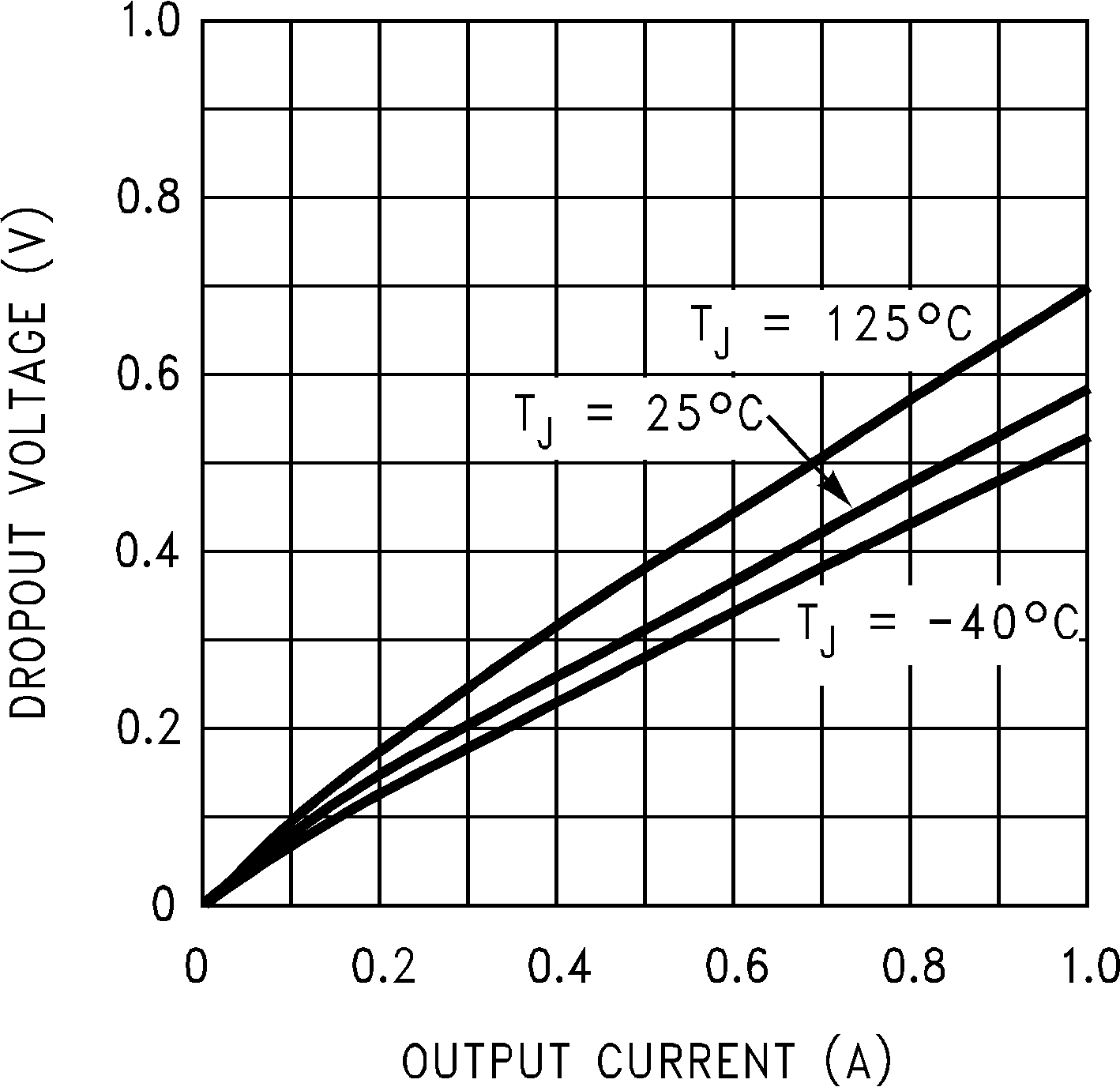
| Dropout voltage | IOUT = 0.1 A, ΔVOUT ≤ 100 mV −40°C ≤ TJ ≤ 125°C |
0.1 | 0.3 | 0.1 | 0.3 | V | ||
| IOUT = 1 A, ΔVOUT ≤ 100 mV −40°C ≤ TJ ≤ 125°C |
0.6 | 1 | 0.6 | 1 | V | |||
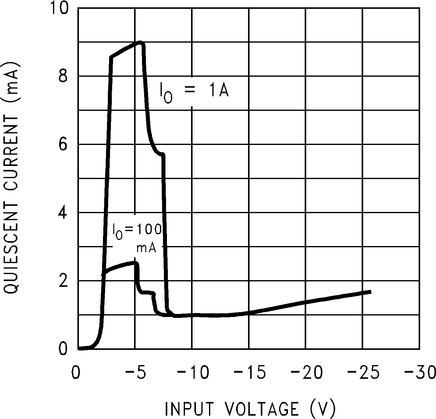
| Quiescent current (Iq) | IOUT ≤ 1 A | 1 | 5 | 1 | 5 | mA | ||
| IOUT = 1 A, VIN = VOUT(NOM) | 9 | 50 | 9 | 50 | ||||
| Short circuit current | RL = 1 Ω(4) | 1.5 | 1.8 | 1.5 | 1.8 | A | ||
| Maximum output current | See(4) | 1.5 | 1.8 | 1.5 | 1.8 | A | ||
| Ripple rejection | Vripple = 1 Vrms, ƒripple = 1 kHz, IOUT = 5 mA |
50 | 58 | 50 | 58 | dB(min) | ||
| Output noise voltage | 10 Hz to 100 kHz, IOUT = 5 mA | 250 | 750 | 250 | 750 | μV(max) | ||
| Long-term stability | 1000 Hours | 2000 | 2000 | ppm | ||||
(1) VOUT(NOM) is the nominal (typical) regulator output voltage, −5 V, −5.2 V, −12 V or −15 V.
(2) Limits are specified and 100% production tested.
(3) Typicals are at TJ = 25°C and represent the most likely parametric norm.
(4) The short circuit current is less than the maximum output current with the −12 V and −15 V versions due to internal foldback current limiting. The −5 V and −5.2 V versions, tested with a lower input voltage, does not reach the foldback current limit and therefore conducts a higher short circuit current level. If the LM2990 output is pulled above ground, the maximum allowed current sunk back into the LM2990 is 1.5 A.
6.6 Electrical Characteristics: –12 V and –15 V
VIN = −5 V + VOUT(NOM)(1), IOUT = 1 A, COUT = 47 μF, unless otherwise specified. All limits apply for TJ = 25°C, unless otherwise indicated in the Test Conditions.| PARAMETER | TEST CONDITIONS | LM2990 –12V | LM2990 –15V | UNIT | ||||
|---|---|---|---|---|---|---|---|---|
| MIN(2) | TYP(3) | MAX(2) | MIN(2) | TYP(3) | MAX(2) | |||
| Output voltage (VOUT) | 5 mA ≤ IOUT ≤ 1 A | −12.24 | –12 | –11.76 | −15.30 | –15 | –14.70 | V |
| 5 mA ≤ IOUT ≤ 1 A −40°C ≤ TJ ≤ 125°C |
–12.60 | –12 | −11.40 | –15.75 | –15 | –14.25 | V | |
| Line regulation | IOUT = 5 mA, VOUT(NOM) −1 V > VIN > −26 V |
6 | 60 | 6 | 60 | mV | ||
| Load regulation | 50 mA ≤ IOUT ≤ 1 A | 3 | 50 | 3 | 50 | mV | ||
| Dropout voltage | IOUT = 0.1 A, ΔVOUT ≤ 100 mV −40°C ≤ TJ ≤ 125°C |
0.1 | 0.3 | 0.1 | 0.3 | V | ||
| IOUT = 1 A, ΔVOUT ≤ 100 mV −40°C ≤ TJ ≤ 125°C |
0.6 | 1 | 0.6 | 1 | V | |||
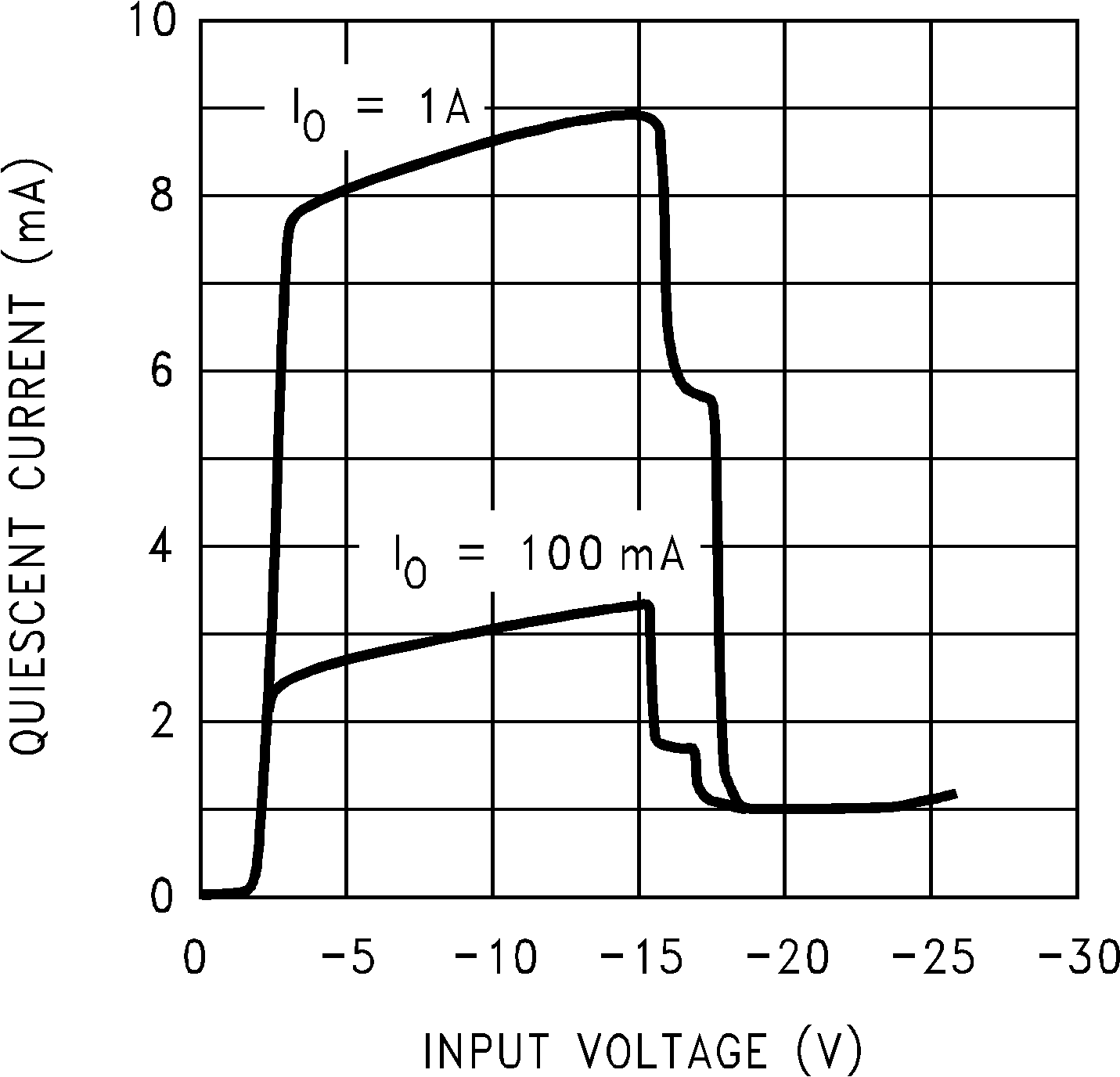
| Quiescent current (Iq) | IOUT ≤ 1 A | 1 | 5 | 1 | 5 | mA | ||
| IOUT = 1 A, VIN = VOUT(NOM) | 9 | 50 | 9 | 50 | ||||
| Short circuit current | RL = 1 Ω(4) | 0.9 | 1.2 | 0.75 | 1.2 | A | ||
| Maximum output current | See(4) | 1.4 | 1.8 | 1.4 | 1.8 | A | ||
| Ripple rejection | Vripple = 1 Vrms, ƒripple = 1 kHz, IOUT = 5 mA |
42 | 52 | 42 | 52 | dB(min) | ||
| Output noise voltage | 10 Hz to 100 kHz, IOUT = 5 mA | 500 | 1500 | 500 | 1500 | μV(max) | ||
| Long-term stability | 1000 hours | 2000 | 2000 | ppm | ||||
(1) VOUT(NOM) is the nominal (typical) regulator output voltage, −5 V, −5.2 V, −12 V or −15 V.
(2) Limits are specified and 100% production tested.
(3) Typicals are at TJ = 25°C and represent the most likely parametric norm.
(4) The short circuit current is less than the maximum output current with the −12 V and −15 V versions due to internal foldback current limiting. The −5 V and −5.2 V versions, tested with a lower input voltage, does not reach the foldback current limit and therefore conducts a higher short circuit current level. If the LM2990 output is pulled above ground, the maximum allowed current sunk back into the LM2990 is 1.5 A.
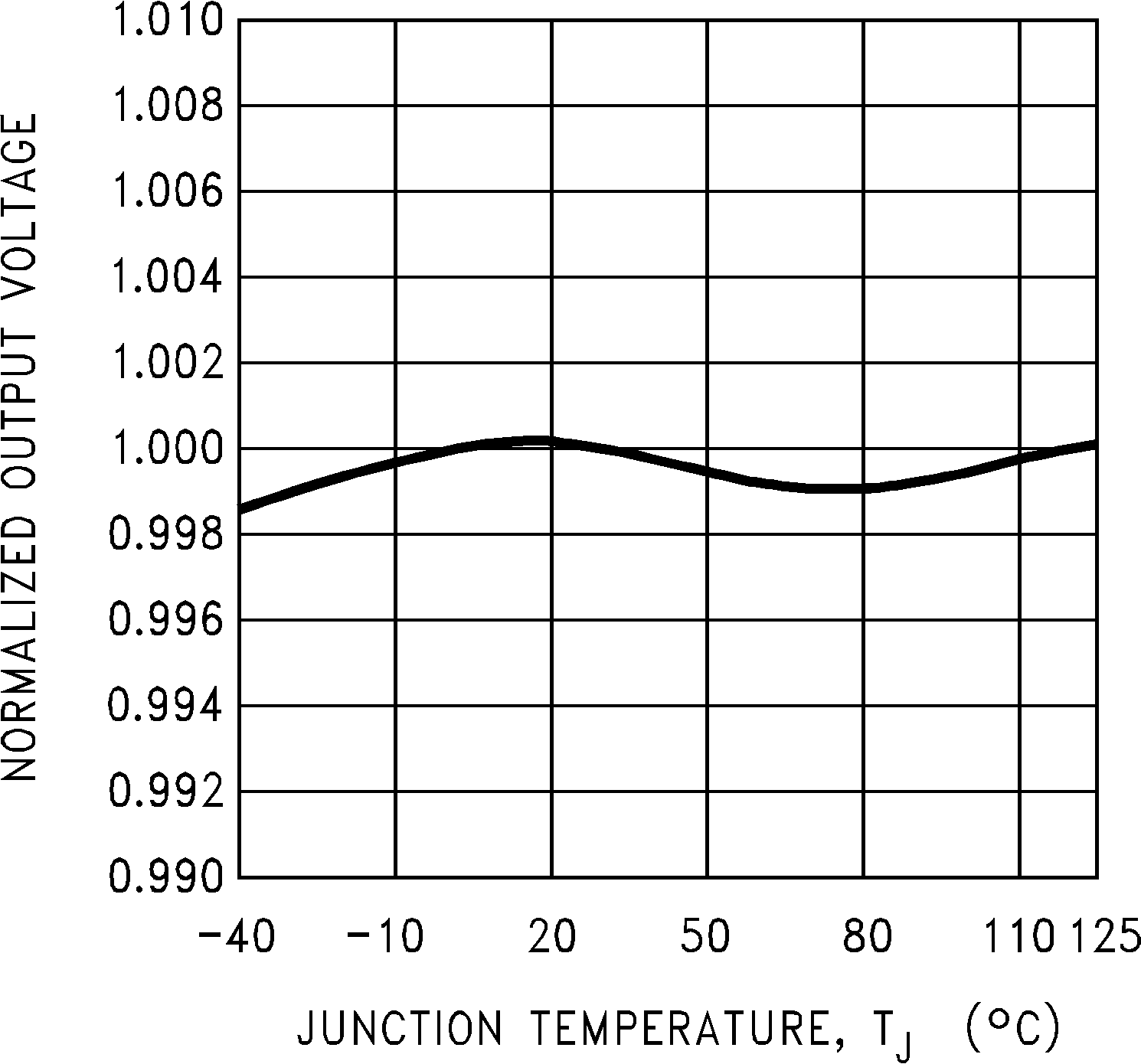
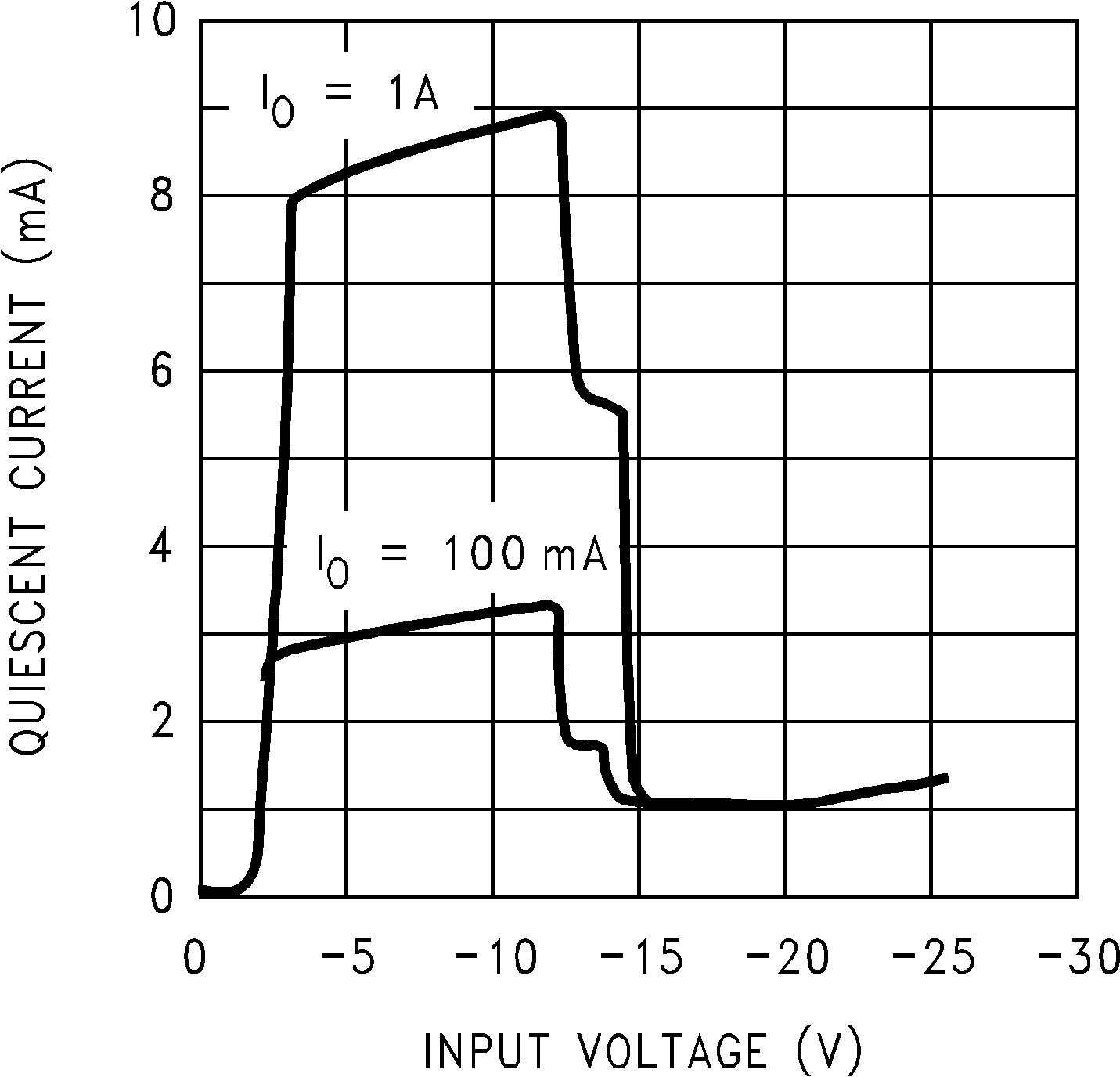
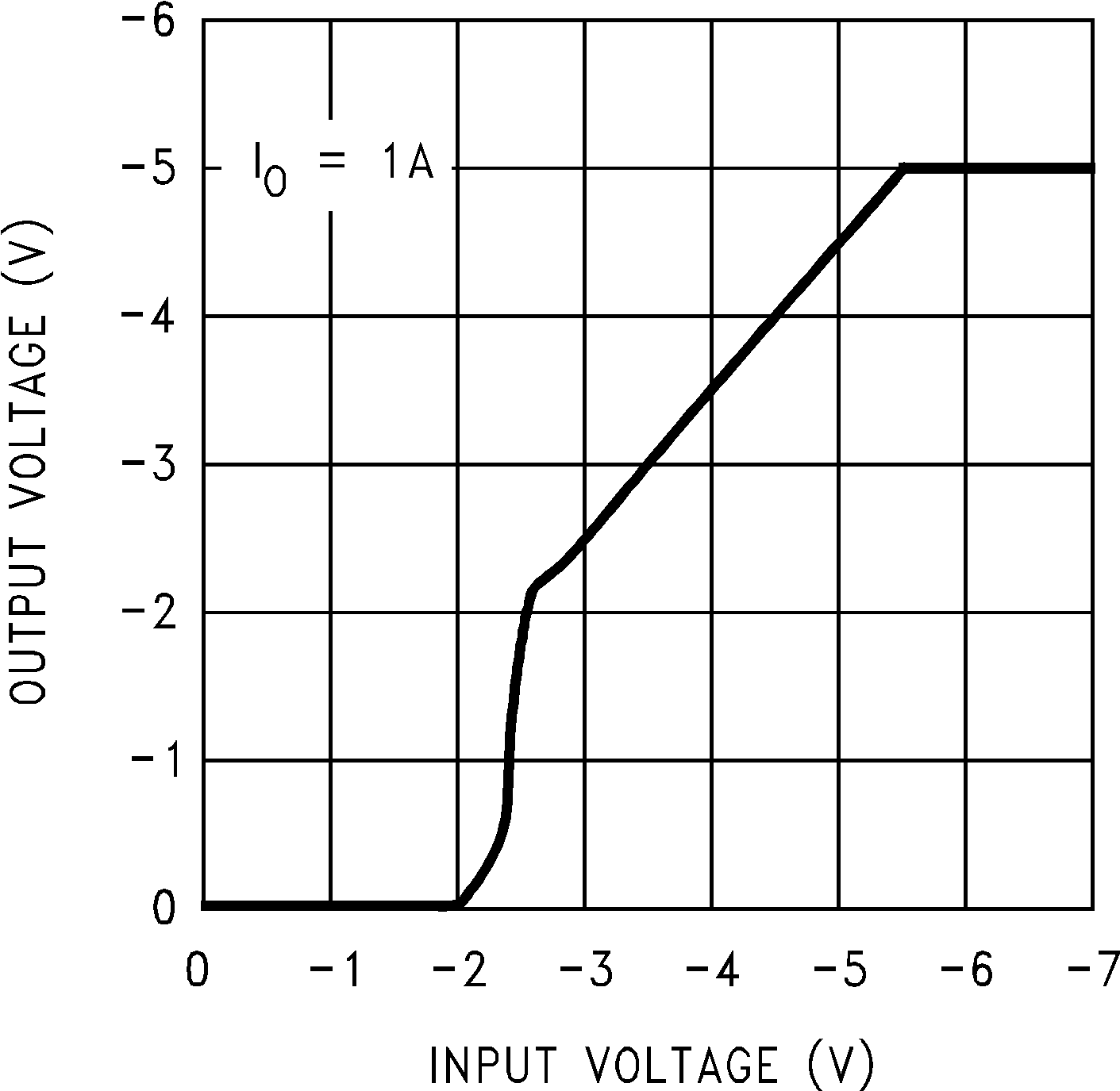
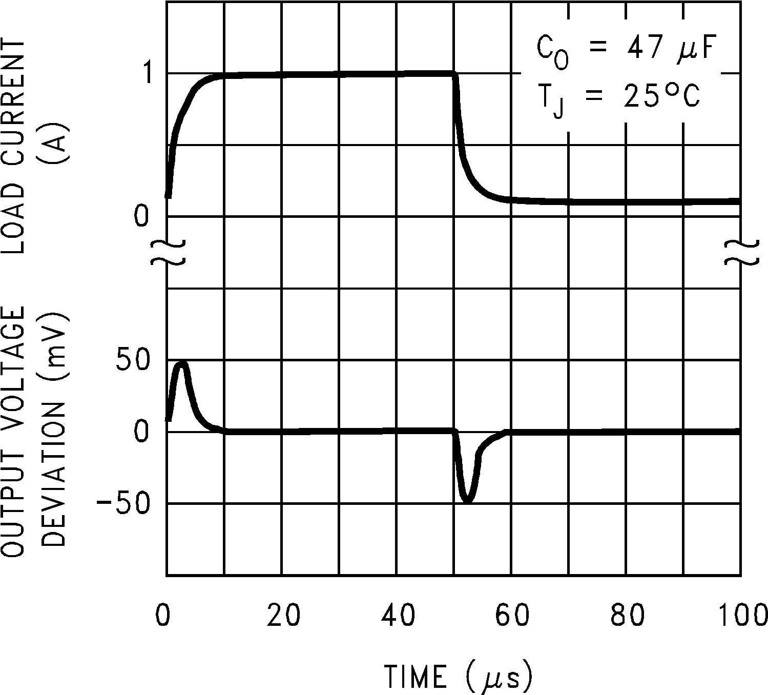
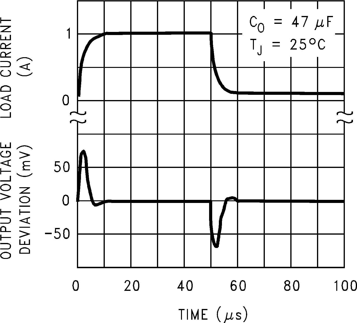
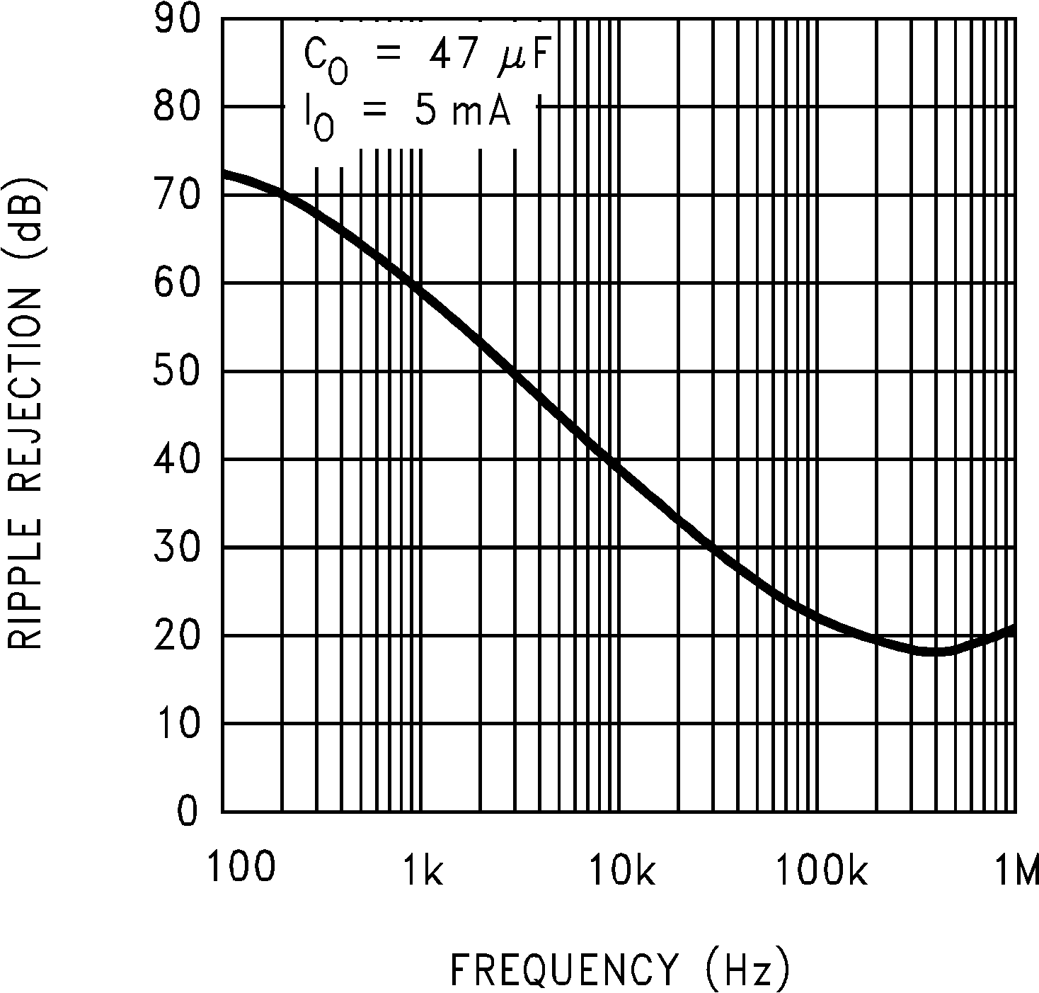
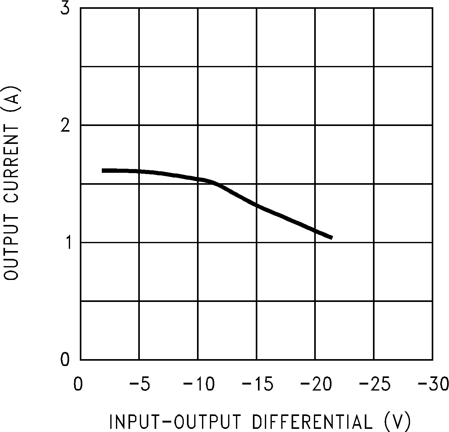
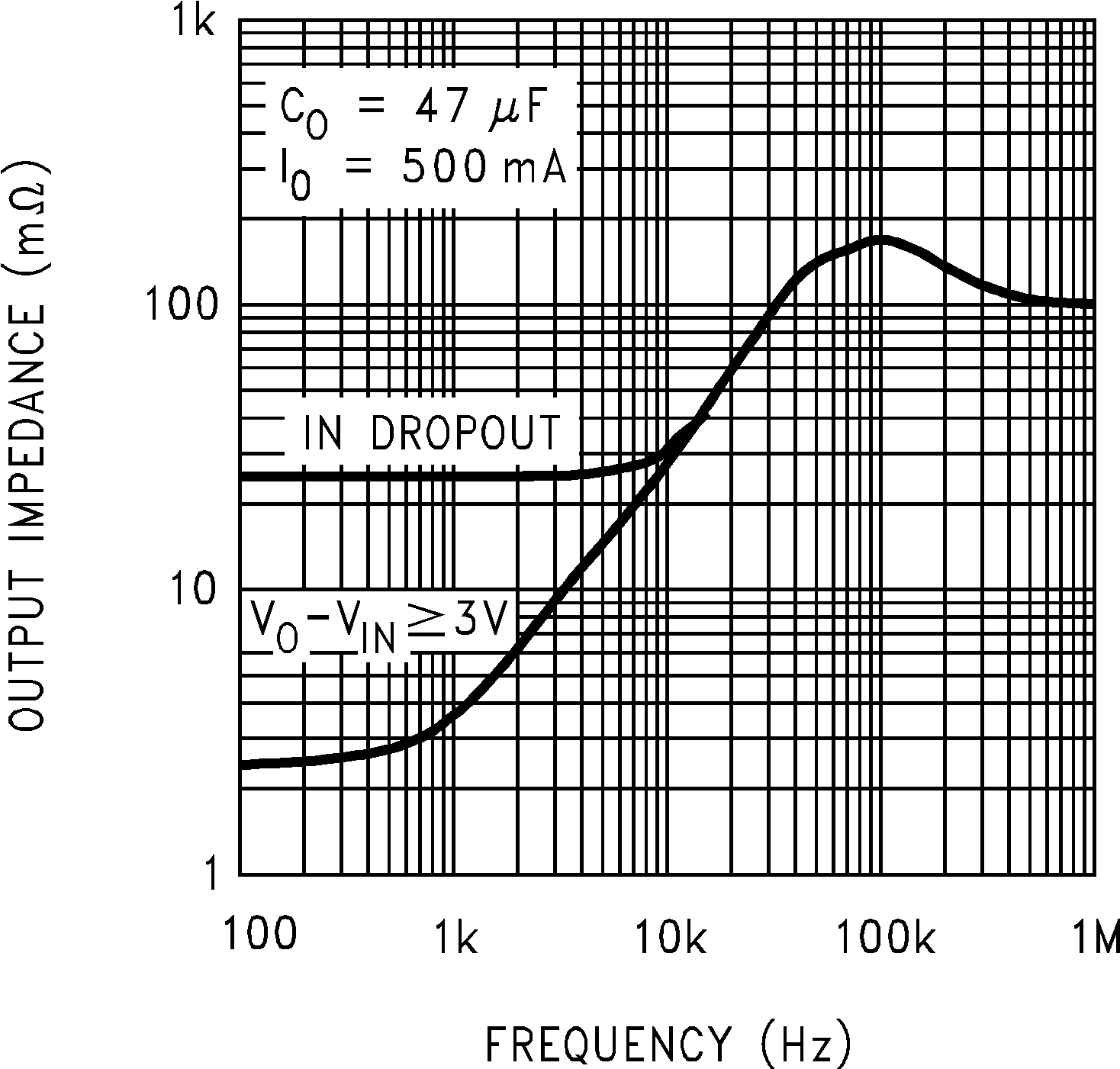
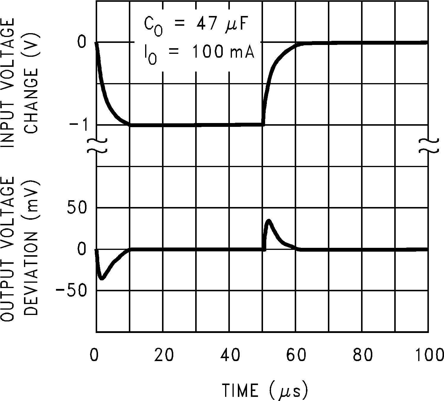
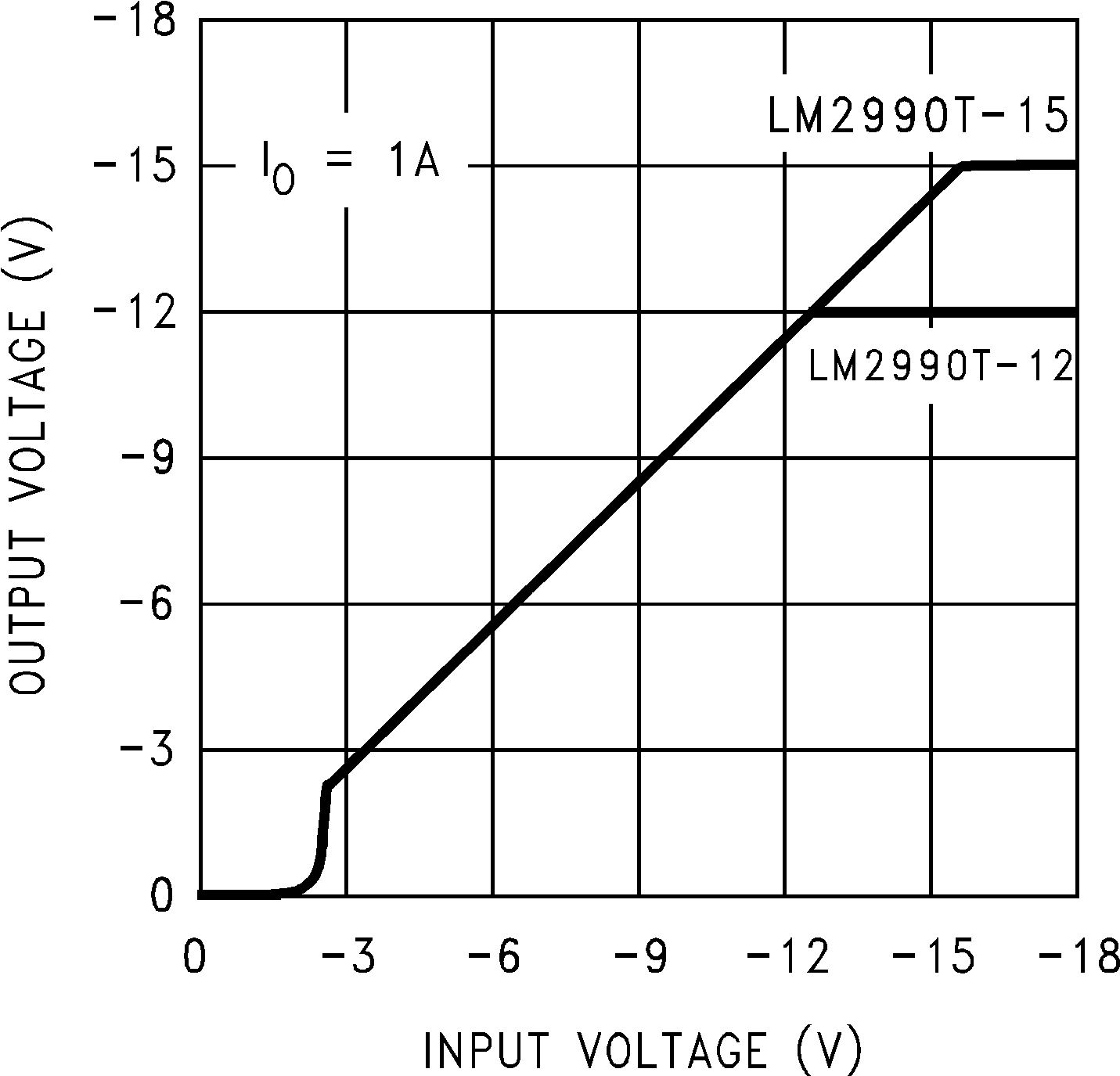
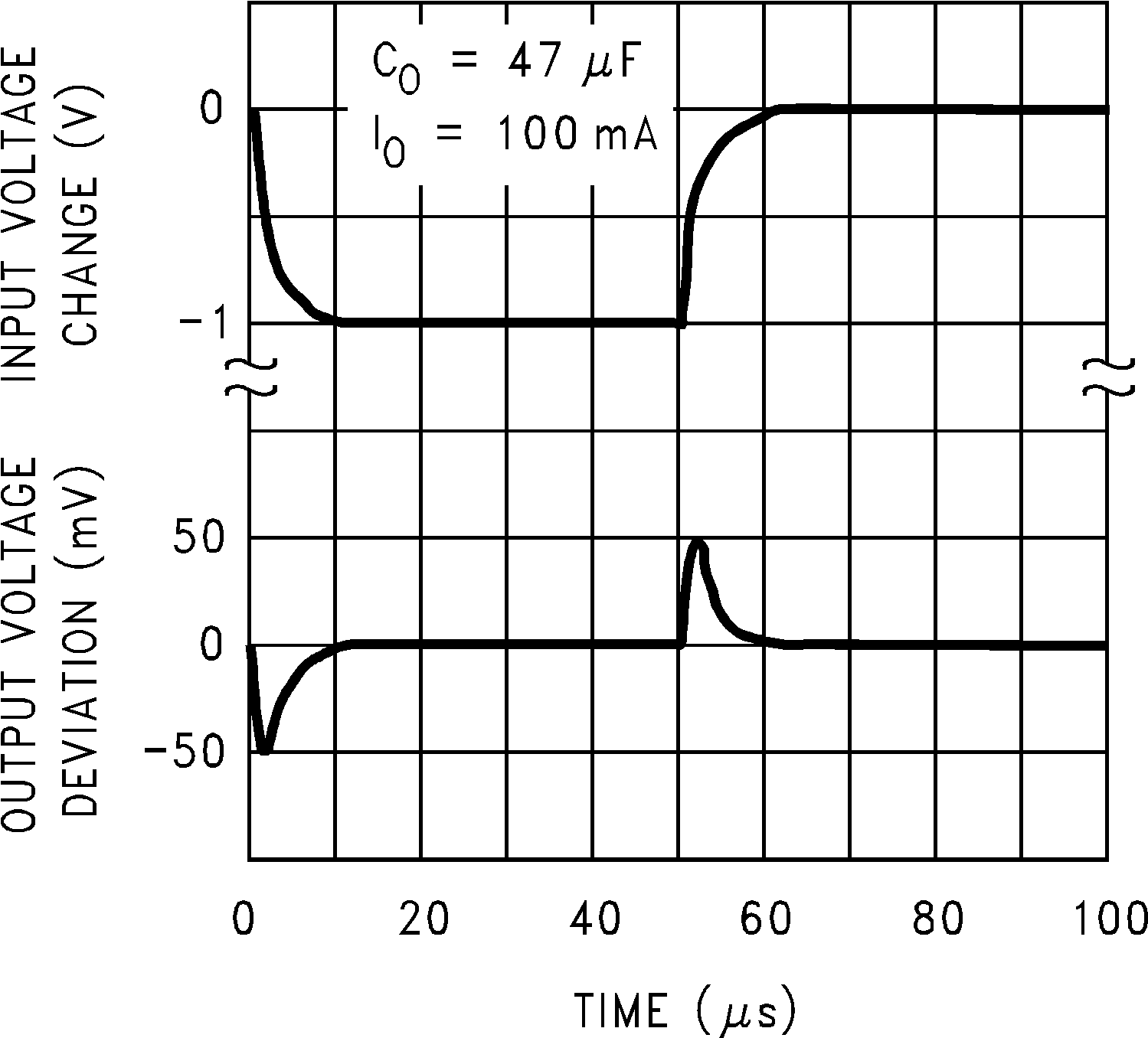
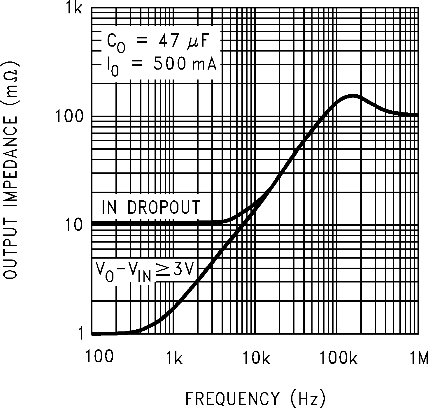
6.7 Typical Characteristics
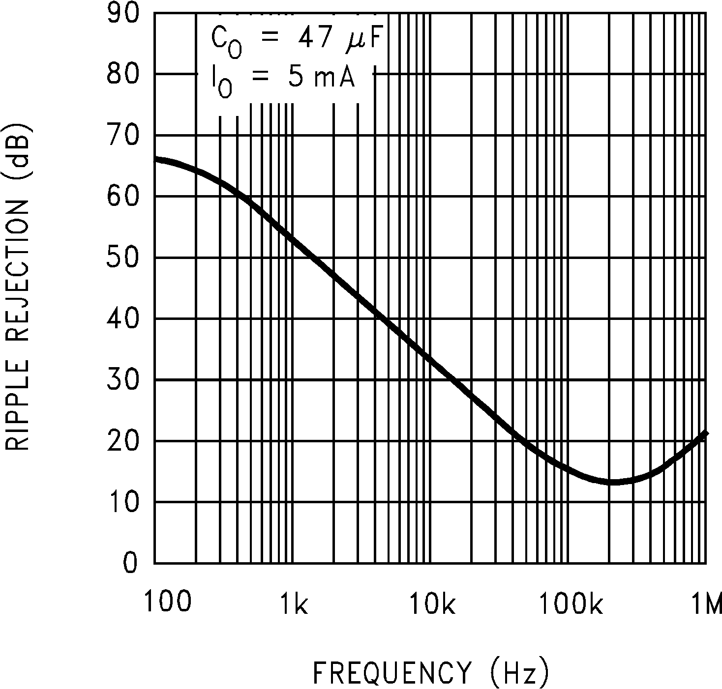
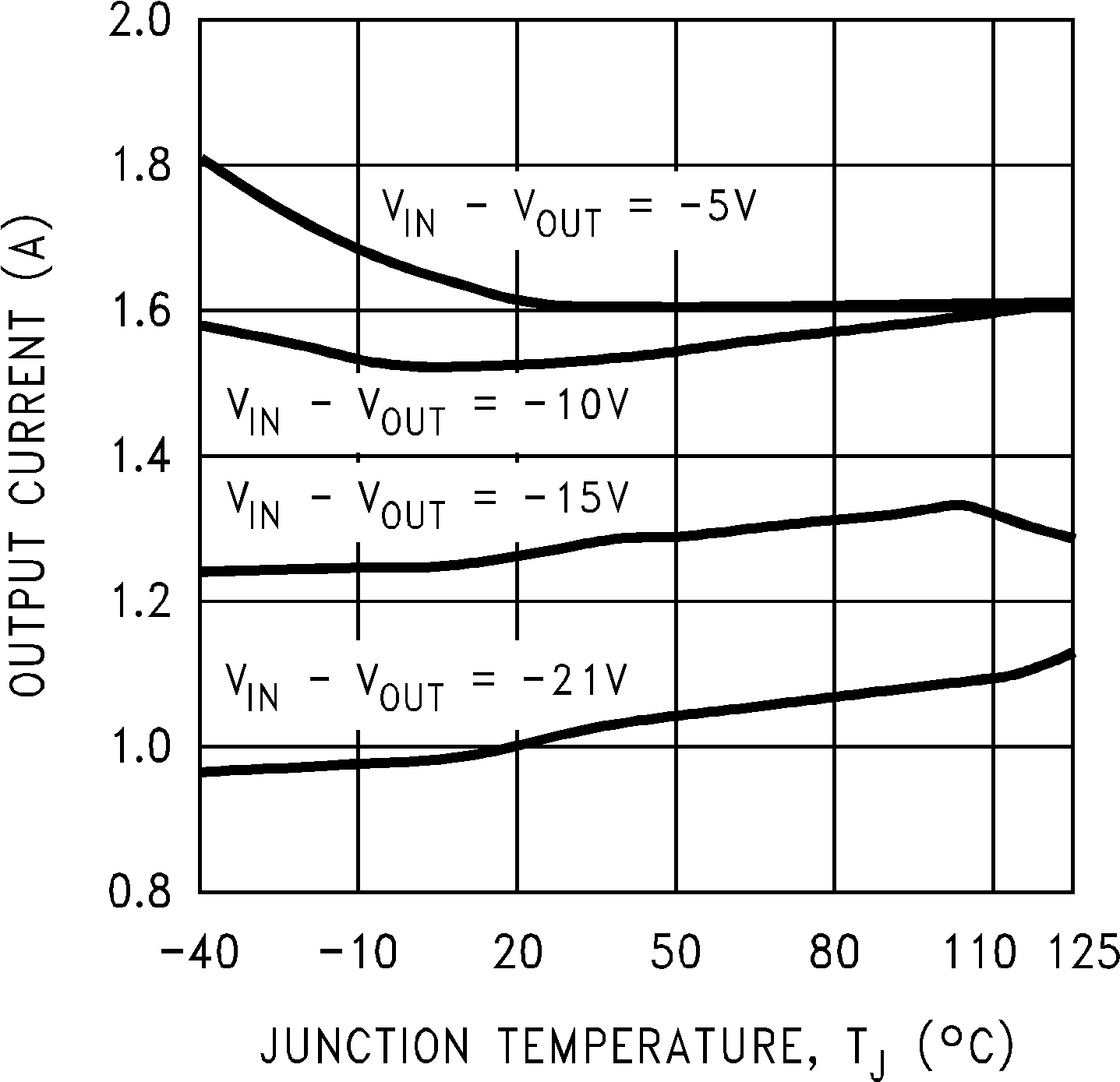
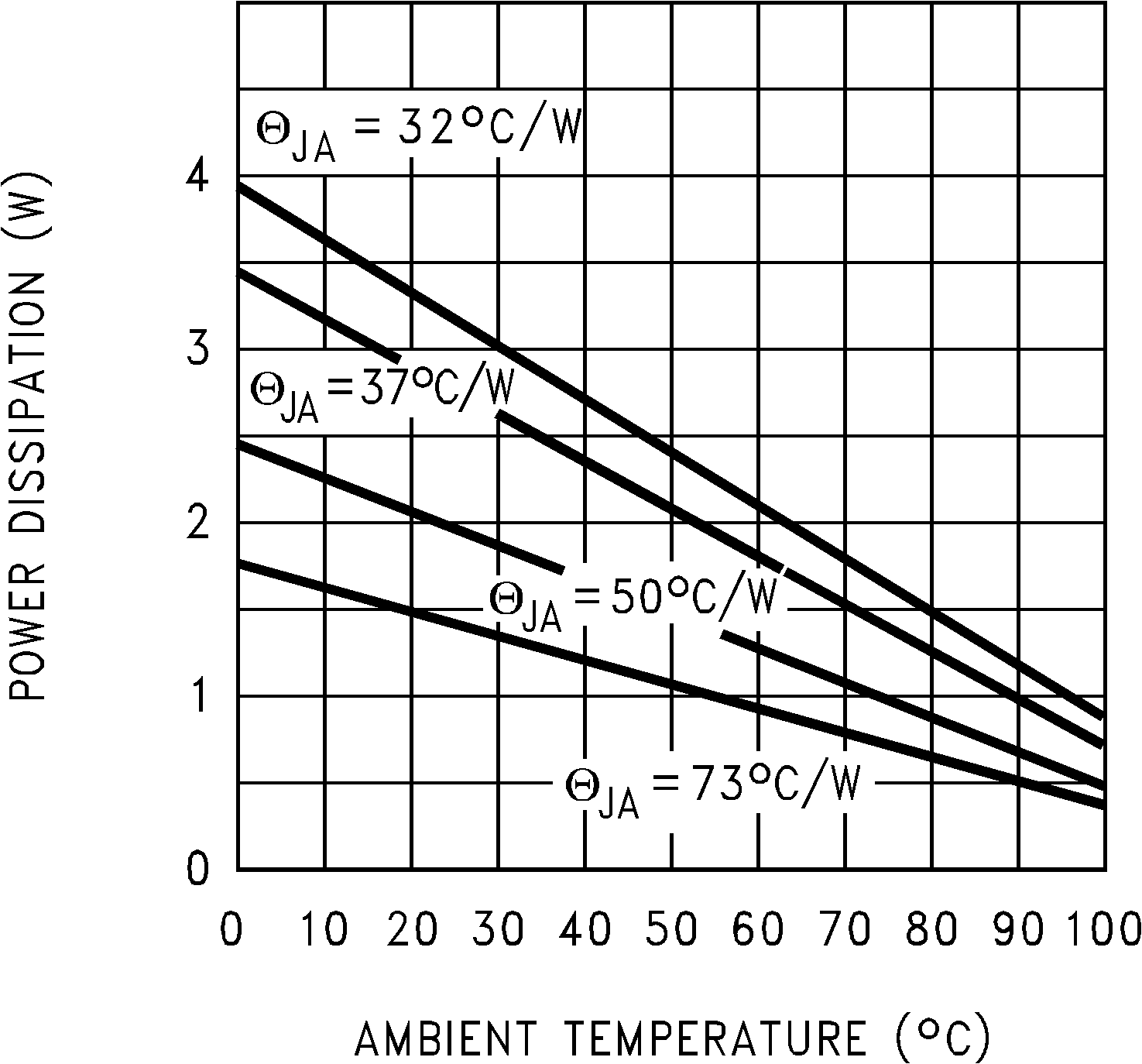
| The maximum power dissipation is a function of TJmax, RθJA, and TA. The maximum allowable power dissipation at any ambient temperature is PD = (TJmax − TA)/RθJA. If this dissipation is exceeded, the die temperature will rise above 125°C, and the LM2990 will eventually go into thermal shutdown at a TJ of approximately 160°C. Please refer to Thermal Information for more details. |
