SNVS421H January 2006 – October 2017 LM3100
PRODUCTION DATA.
- 1 Features
- 2 Applications
- 3 Description
- 4 Revision History
- 5 Pin Configuration and Functions
- 6 Specifications
- 7 Detailed Description
- 8 Applications and Implementation
- 9 Layout
- 10Device and Documentation Support
- 11Mechanical, Packaging, and Orderable Information
Package Options
Mechanical Data (Package|Pins)
- PWP|20
Thermal pad, mechanical data (Package|Pins)
- PWP|20
Orderable Information
8 Applications and Implementation
NOTE
Information in the following applications sections is not part of the TI component specification, and TI does not warrant its accuracy or completeness. TI’s customers are responsible for determining suitability of components for their purposes. Customers should validate and test their design implementation to confirm system functionality.
8.1 Applications Information
8.1.1 External Components
The following guidelines can be used to select the external components.
8.1.1.1 RFB1 and RFB2
The ratio of these resistors is calculated from:

RFB1 and RFB2 should be chosen from standard value resistors in the range of 1.0 kΩ - 10 kΩ which satisfy the above ratio.
For VOUT = 0.8 V, the FB pin can be connected to the output directly. However, the converter operation needs a minimum inductor current ripple to maintain good regulation when no load is connected. This minimum load is about 10 µA and can be implemented by adding a pre-load resistor to the output.
8.1.1.2 RON
The minimum value for RON is calculated from:

Equation 2 in Hysteretic Control Circuit Overview section can be used to select RON if a specific frequency is desired as long as the above limitation is met.
8.1.1.3 L
The main parameter affected by the inductor is the output current ripple amplitude (IOR). The maximum allowable (IOR) must be determined at both the minimum and maximum nominal load currents. At minimum load current, the lower peak must not reach 0 A. At maximum load current, the upper peak must not exceed the current limit threshold (1.9 A). The allowable ripple current is calculated from the following equations:
or
The lesser of the two ripple amplitudes calculated above is then used in the following equation:

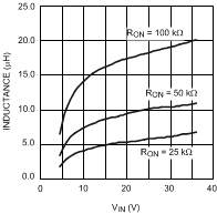
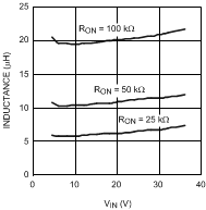
where VIN is the maximum input voltage and Fs is determined from Equation 1. This provides a value for L. The next larger standard value should be used. L should be rated for the IPK current level shown in Figure 20.
 Figure 22. Inductor Selector for VOUT = 3.3 V
 Figure 23. Inductor Selector for VOUT = 0.8 V
8.1.1.4 CVCC
The capacitor on the VCC output provides not only noise filtering and stability, but also prevents false triggering of the VCC UVLO at the buck switch on/off transitions. For this reason, CVCC should be no smaller than 680 nF for stability, and should be a good quality, low ESR, ceramic capacitor.
8.1.1.5 CO and CO3
CO should generally be no smaller than 10 µF. Experimentation is usually necessary to determine the minimum value for CO, as the nature of the load may require a larger value. A load which creates significant transients requires a larger value for CO than a fixed load.
CO3 is a small value ceramic capacitor to further suppress high frequency noise at VOUT. A 47 nF is recommended, located close to the LM3100.
8.1.1.6 CIN and CIN3
CIN’s purpose is to supply most of the switch current during the on-time, and limit the voltage ripple at VIN, assume the voltage source feeding VIN has an output impedance greater than zero. If the source’s dynamic impedance is high (effectively a current source), CIN supplies the average input current, but not the ripple current.
At maximum load current, when the buck switch turns on, the current into VIN suddenly increases to the lower peak of the inductor’s ripple current, ramps up to the peak value, then drop to zero at turn-off. The average current during the on-time is the load current. For a worst case calculation, CIN must supply this average load current during the maximum on-time. CIN is calculated from:

where IOUT is the load current, tON is the maximum on-time, and ΔV is the allowable ripple voltage at VIN.
CIN3’s purpose is to help avoid transients and ringing due to long lead inductance at VIN. A low ESR, 0.1 µF ceramic chip capacitor is recommended, located close to the LM3100.
8.1.1.7 CBST
The recommended value for CBST is 33 nF. A high quality ceramic capacitor with low ESR is recommended as CBST supplies a surge current to charge the buck switch gate at turn-on. A low ESR also helps ensure a complete recharge during each off-time.
8.1.1.8 CSS
The capacitor at the SS pin determines the soft-start time, i.e. the time for the reference voltage at the regulation comparator, and the output voltage, to reach their final value. The time is determined from the following:

8.1.1.9 CFB
If output voltage is higher than 1.6 V, this feedback capacitor is needed for Discontinuous Conduction Mode to improve the output ripple performance, the recommended value for CFB is 10 nF.

