SNVS421H January 2006 – October 2017 LM3100
PRODUCTION DATA.
- 1 Features
- 2 Applications
- 3 Description
- 4 Revision History
- 5 Pin Configuration and Functions
- 6 Specifications
- 7 Detailed Description
- 8 Applications and Implementation
- 9 Layout
- 10Device and Documentation Support
- 11Mechanical, Packaging, and Orderable Information
Package Options
Mechanical Data (Package|Pins)
- PWP|20
Thermal pad, mechanical data (Package|Pins)
- PWP|20
Orderable Information
6 Specifications
6.1 Absolute Maximum Ratings
over operating free-air temperature range (unless otherwise noted)(1)(2)| MIN | MAX | UNIT | ||
|---|---|---|---|---|
| VIN, RON to GND | –0.3 | 40 | V | |
| SW to GND | –0.3 | 40 | V | |
| SW to GND (Transient) | –2 | (< 100 ns) | V | |
| VIN to SW | –0.3 | 40 | V | |
| BST to SW | –0.3 | 7 | V | |
| All Other Inputs to GND | –0.3 | 7 | V | |
| Junction Temperature, TJ | –65 | 150 | °C | |
| Storage temperature, Tstg | 150 | °C | ||
(1) Stresses beyond those listed under Absolute Maximum Ratings may cause permanent damage to the device. These are stress ratings only, which do not imply functional operation of the device at these or any other conditions beyond those indicated under Recommended Operating Conditions. Exposure to absolute-maximum-rated conditions for extended periods may affect device reliability.
(2) Military/Aerospace specified devices are required, please contact the Texas Instruments Sales Office/ Distributors for availability and specifications.
6.2 ESD Ratings
| VALUE | UNIT | |||
|---|---|---|---|---|
| V(ESD) | Electrostatic discharge | Human-body model (HBM), per ANSI/ESDA/JEDEC JS-001(1)(2) | ±2 | kV |
(1) JEDEC document JEP155 states that 500-V HBM allows safe manufacturing with a standard ESD control process.
(2) The human body model is a 100-pF capacitor discharged through a 1.5-kΩ resistor into each pin.
6.3 Recommended Operating Conditions
over operating free-air temperature range (unless otherwise noted)| MIN | MAX | UNIT | ||
|---|---|---|---|---|
| Supply Voltage Range VIN | 4.5 | 36 | V | |
| Junction Temperature Range TJ | –40 | 125 | °C | |
6.4 Thermal Information
| THERMAL METRIC(1) | LM3100 | UNIT | |
|---|---|---|---|
| PWP (HTSSOP) | |||
| 20 PINS | |||
| RθJC | Junction-to-case thermal resistance | 6.5 | °C/W |
(1) For more information about traditional and new thermal metrics, see the Semiconductor and IC Package Thermal Metrics application report.
6.5 Electrical Characteristics
at TJ = 25°C, and VIN = 18 V, VOUT = 3.3 V (unless otherwise noted).(1)| PARAMETER | TEST CONDITIONS | MIN | TYP | MAX | UNIT | ||
|---|---|---|---|---|---|---|---|
| START-UP REGULATOR, VCC | |||||||
| VCC | Output voltage | CCC = 680 nF, no load | TJ = –40°C to 125°C | 5.0 | 6.0 | 7.2 | V |
| VIN - VCC | Dropout voltage | ICC = 2 mA | TJ = –40°C to 125°C | 50 | 140 | mV | |
| ICC = 20 mA | TJ = –40°C to 125°C | 350 | 570 | ||||
| IVCCL | Current limit(1) | VCC = 0 V | TJ = –40°C to 125°C | 40 | 65 | mA | |
| VCC-UVLO | Under-voltage lockout threshold | VIN increasing | TJ = –40°C to 125°C | 3.6 | 3.75 | 3.85 | V |
| VCC-UVLO-HYS | UVLO hysteresis | VIN decreasing | 130 | mV | |||
| tVCC-UVLO-D | UVLO filter delay | 3 | µs | ||||
| IIN | Operating current | No switching, VFB = 1 V | TJ = –40°C to 125°C | 0.7 | 1 | mA | |
| IIN-SD | Operating current, Device shutdown | VEN = 0 V | TJ = –40°C to 125°C | 17 | 30 | µA | |
| SWITCHING CHARACTERISTICS | |||||||
| RDS-UP-ON | Main MOSFET Rds(on) | TJ = –40°C to 125°C | 0.18 | 0.35 | Ω | ||
| RDS- DN-ON | Syn. MOSFET Rds(on) | TJ = –40°C to 125°C | 0.11 | 0.2 | Ω | ||
| VG-UVLO | Gate drive voltage UVLO | VBST - VSW increasing | TJ = –40°C to 125°C | 3.3 | 4 | V | |
| SOFT-START | |||||||
| ISS | SS pin source current | VSS = 0.5 V | TJ = –40°C to 125°C | 6 | 8 | 9.8 | µA |
| CURRENT LIMIT | |||||||
| ICL | Syn. MOSFET current limit threshold | 1.9 | A | ||||
| ON/OFF TIMER | |||||||
| tON | ON timer pulse width | VIN = 10 V, RON = 100 kΩ | 1.38 | µs | |||
| VIN = 30 V, RON = 100 kΩ | 0.47 | ||||||
| tON-MIN | ON timer minimum pulse width | 200 | ns | ||||
| tOFF | OFF timer pulse width | 260 | ns | ||||
| ENABLE INPUT | |||||||
| VEN | EN Pin input threshold | VEN rising | TJ = –40°C to 125°C | 1.236 | 1.26 | 1.285 | V |
| VEN-HYS | Enable threshold hysteresis | VEN falling | 90 | mV | |||
| REGULATION and OVER-VOLTAGE COMPARATOR | |||||||
| VFB | In-regulation feedback voltage | VSS ≥ 0.8 V | TJ = –40°C to 125°C | 0.784 | 0.8 | 0.816 | V |
| VSS ≥ 0.8 V | TJ = –40°C to 125°C | 0.788 | 0.812 | ||||
| VFB-OV | Feedback over-voltage threshold | TJ = –40°C to 125°C | 0.894 | 0.920 | 0.940 | V | |
| IFB | TJ = –40°C to 125°C | 5 | 100 | nA | |||
| THERMAL SHUTDOWN | |||||||
| TSD | Thermal shutdown temperature | TJ rising | 165 | °C | |||
| TSD-HYS | Thermal shutdown temperature hysteresis | TJ falling | 20 | °C | |||
(1) VCC provides self bias for the internal gate drive and control circuits. Device thermal limitations limit external loading.
6.6 Typical Characteristics
All curves taken at VIN = 18 V with configuration in typical application circuit for VOUT = 3.3 V shown in this datasheet. TA = 25°C, unless otherwise specified.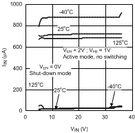
1.
Figure 1. Quiescent Current, IIN vs VIN
1.
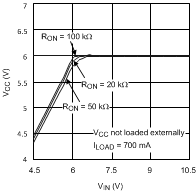
Figure 3. VCC vs VIN
1.
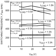
Figure 5. Switching Frequency, FSW vs VIN
1.
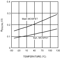
Figure 7. RDS(ON) vs Temperature
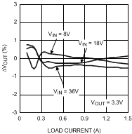
1.
Figure 9. VOUT Regulation vs Load Current
| VOUT = 3.3 V |
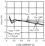
1.
Figure 11. VOUT Regulation vs Load Current
| VOUT = 0.8 V |
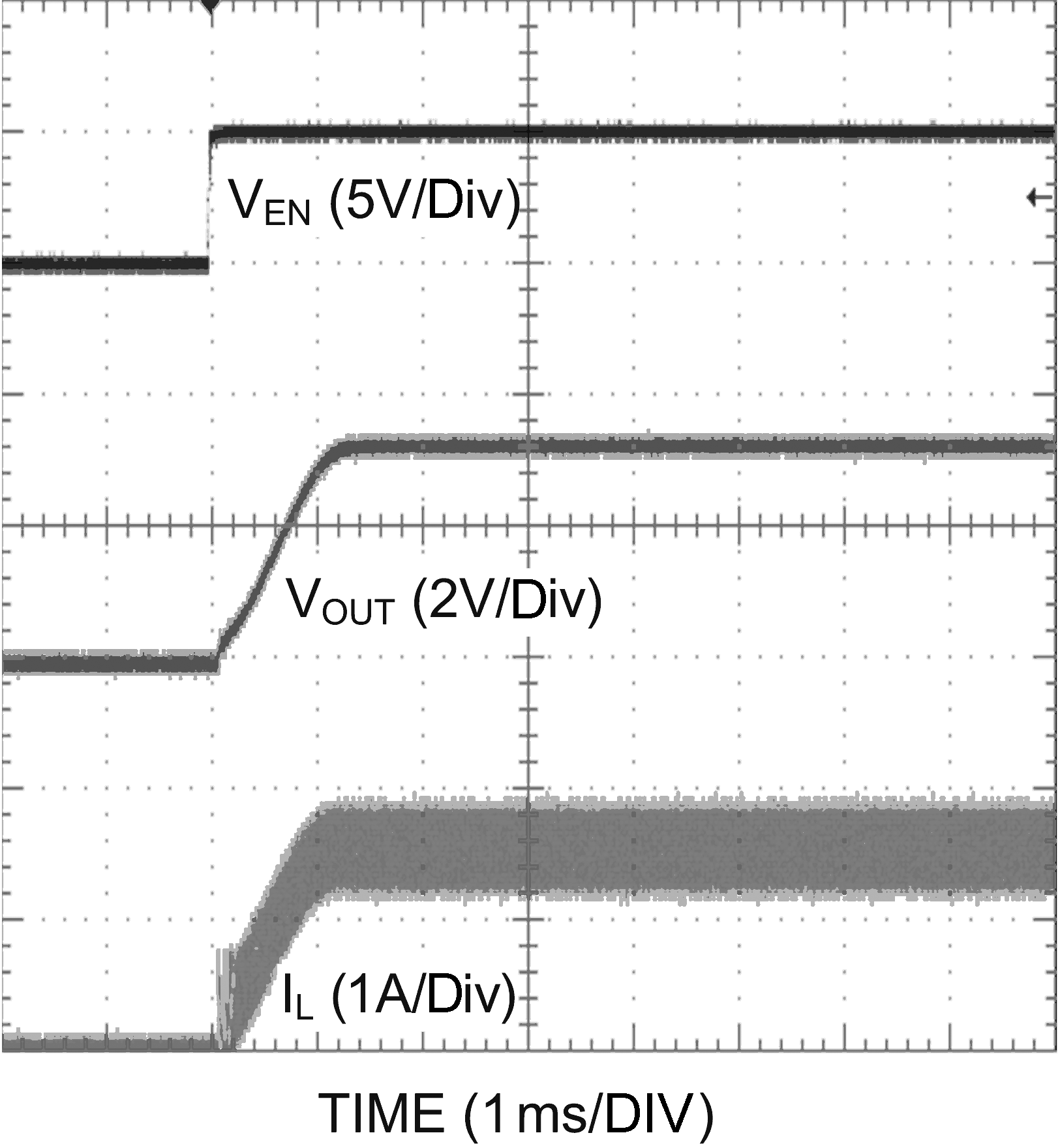
1.
Figure 13. Enable Transient
| VOUT = 3.3 V, 1.5 A Loaded |
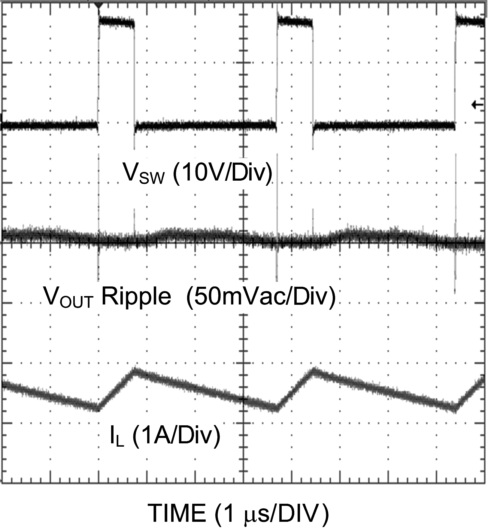
1.
Figure 15. Continuous Mode Operation
| VOUT = 3.3 V, 1.5 A Loaded |
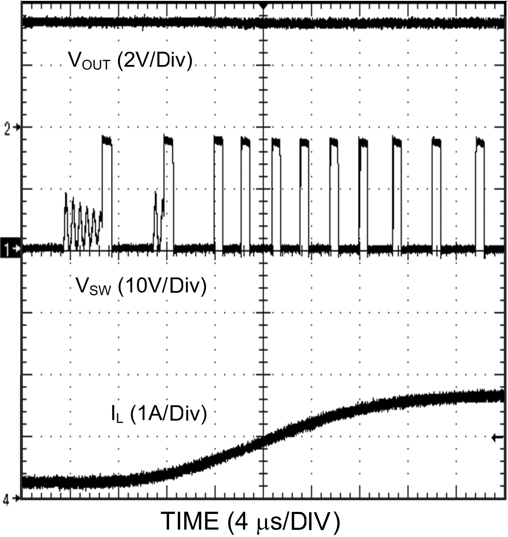
1.
Figure 17. CCM to DCM Transition
| VOUT = 3.3 V, 0.15 A - 1.5 A Load |
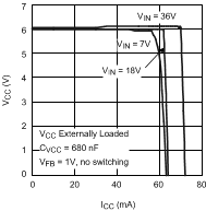
1.
Figure 2. VCC vs ICC
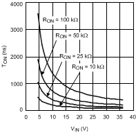
1.
Figure 4. TON vs VIN
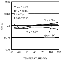
1.
Figure 6. VFB vs Temperature
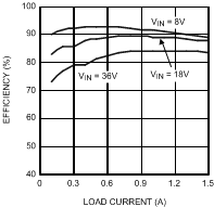
1.
Figure 8. Efficiency vs Load Current
| VOUT = 3.3 V | ||
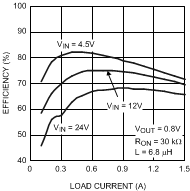
1.
Figure 10. Efficiency vs Load Current
| VOUT = 0.8 V |
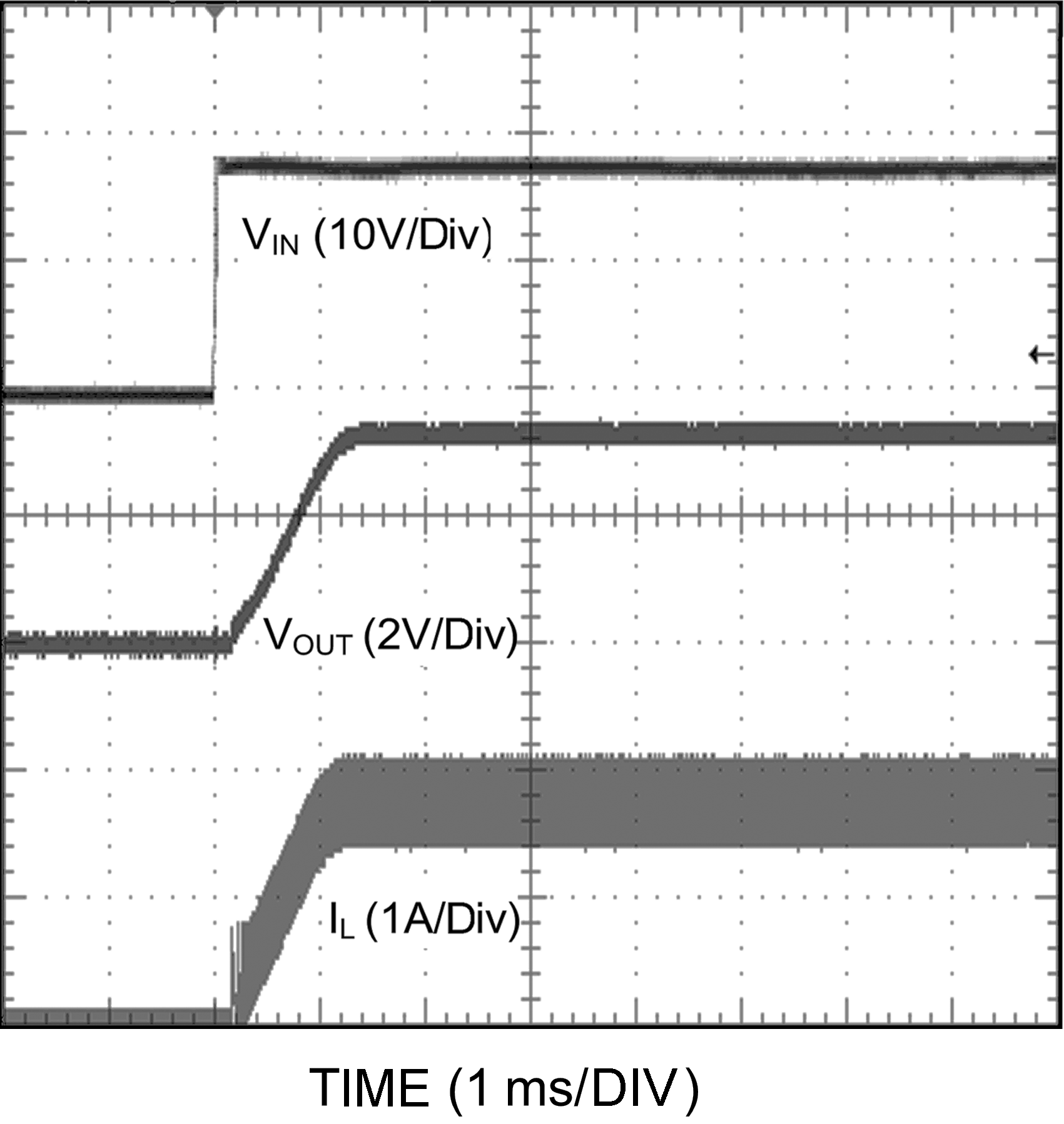
1.
Figure 12. Power Up
| VOUT = 3.3 V, 1.5 A Loaded | ||
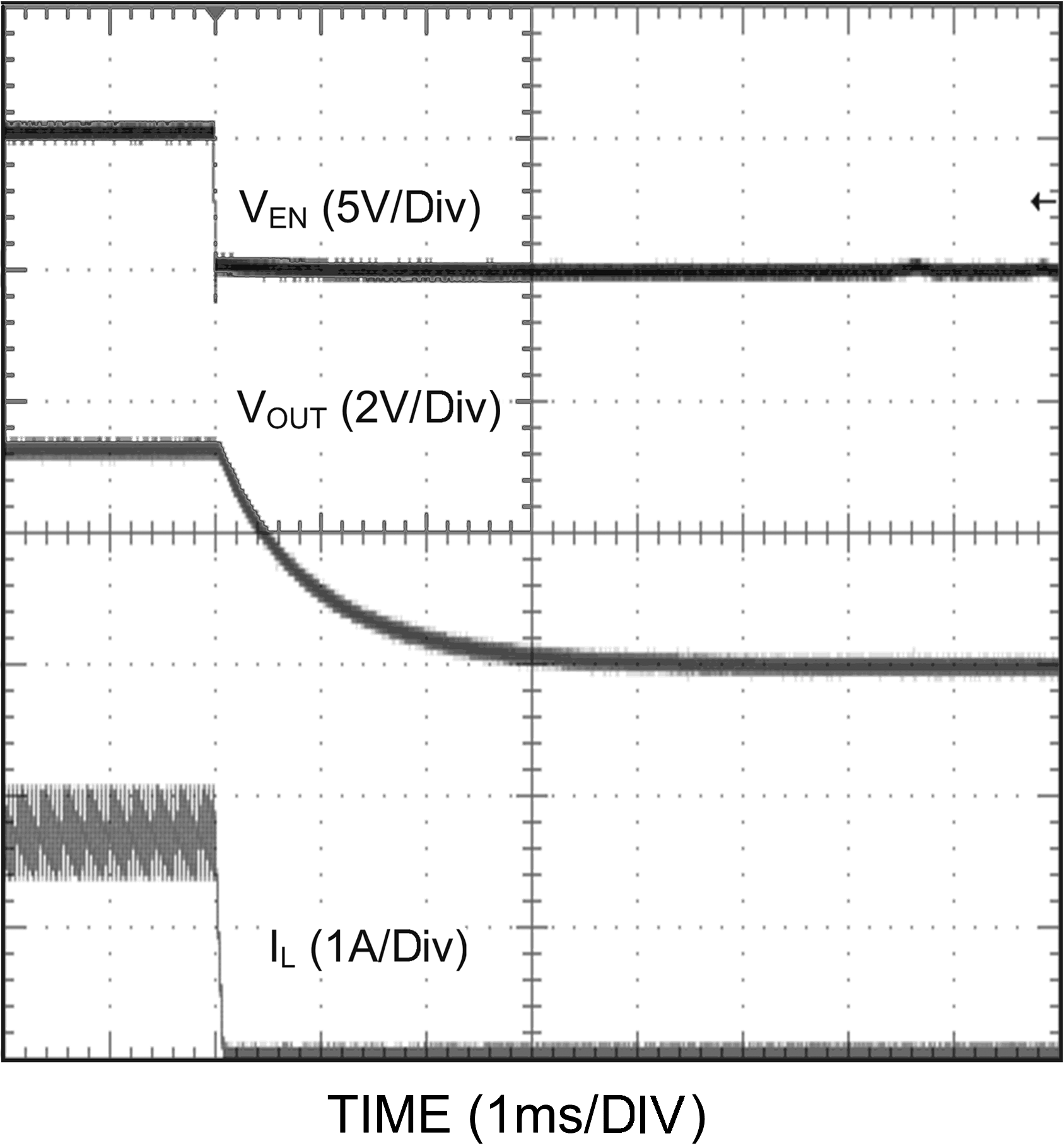
1.
Figure 14. Shutdown Transient
| VOUT = 3.3 V, 1.5 A Loaded |
1.
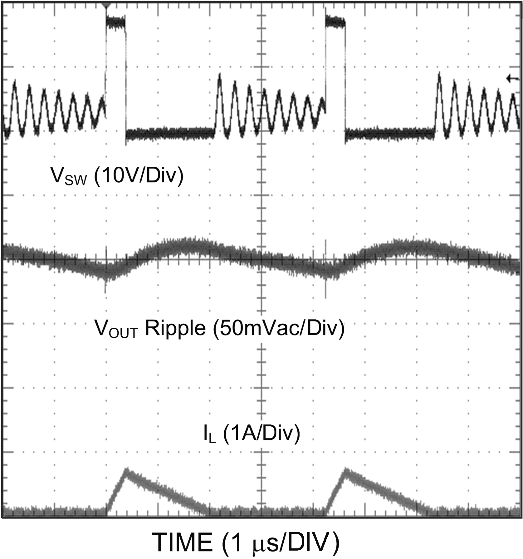
Figure 16. Discontinuous Mode Operation
| VOUT = 3.3 V, 0.15 A Loaded |
1.
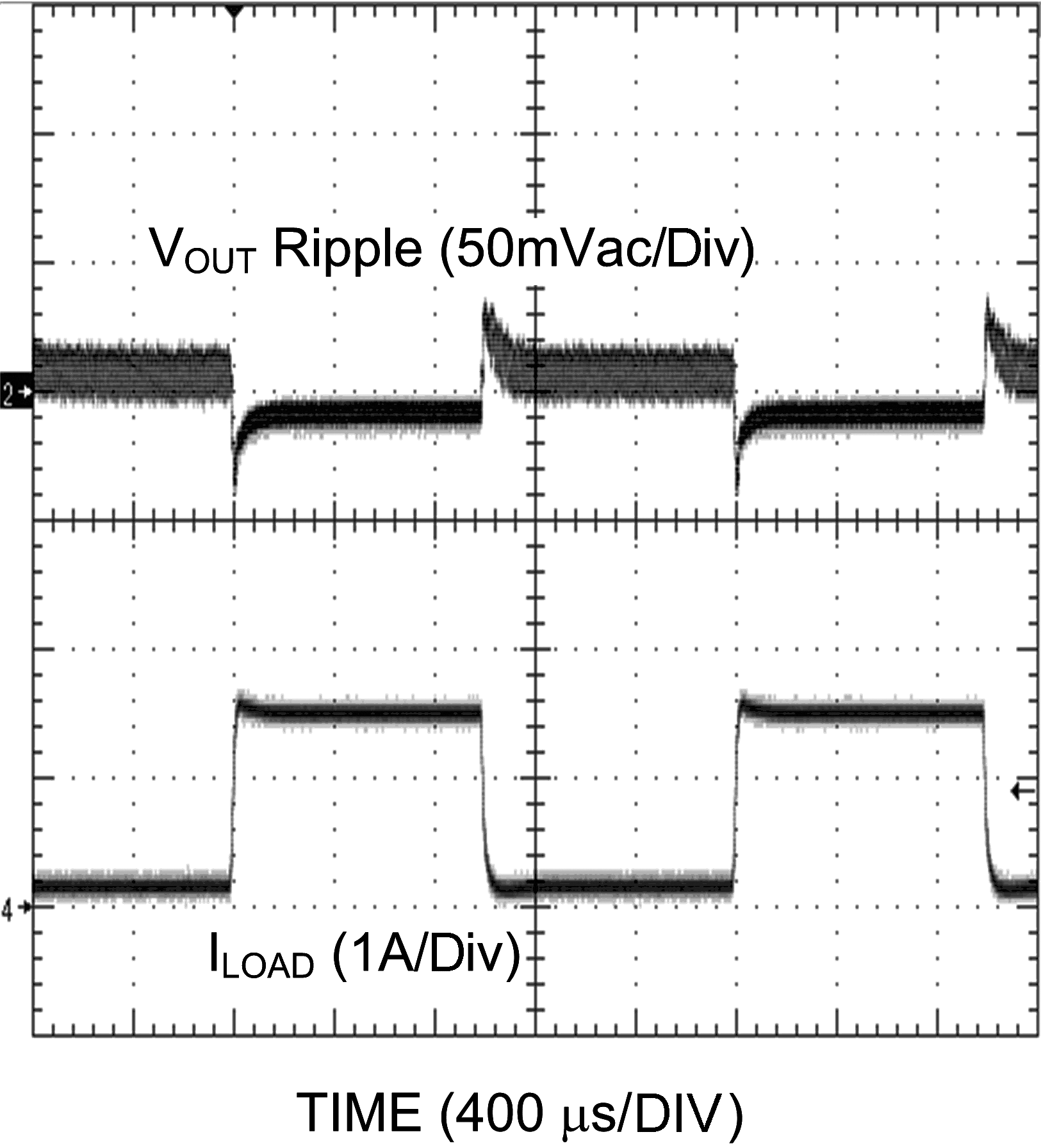
Figure 18. Load Transient
| VOUT = 3.3 V, 0.15 A - 1.5 A Load | Current slew-rate: 2.5 A/µs | |