SNVS561G September 2008 – September 2015 LM3150
PRODUCTION DATA.
- 1 Features
- 2 Applications
- 3 Description
- 4 Typical Application Schematic
- 5 Revision History
- 6 Pin Configuration and Functions
- 7 Specifications
- 8 Detailed Description
- 9 Application and Implementation
- 10Power Supply Recommendations
- 11Layout
- 12Device and Documentation Support
- 13Mechanical, Packaging, and Orderable Information
Package Options
Mechanical Data (Package|Pins)
- PWP|14
Thermal pad, mechanical data (Package|Pins)
- PWP|14
Orderable Information
8 Detailed Description
8.1 Overview
The LM3150 synchronous step-down controller uses a COT architecture which is a derivative of the hysteretic control scheme. COT relies on a fixed switch on-time to regulate the output. The on-time of the high-side switch can be set manually by adjusting the size of an external resistor (RON). To maintain a relatively constant switching frequency as VIN varies, the LM3150 controller automatically adjusts the on-time inversely with the input voltage. Assuming an ideal system and VIN is much greater than 1 V, the following approximations can be made:
The on-time, tON:

where
- constant K = 100 pC
The RON resistance value can be calculated as follows:

where
- fs is the desired switching frequency
Control is based on a comparator and the on-timer, with the output voltage feedback (FB) compared with an internal reference of 0.6 V. If the FB level is below the reference, the high-side switch is turned on for a fixed time, tON, which is determined by the input voltage and the resistor RON. Following this on-time, the switch remains off for a minimum off-time, tOFF, as specified in the Electrical Characteristics table or until the FB pin voltage is below the reference, then the switch turns on again for another on-time period. The switching will continue in this fashion to maintain regulation. During continuous conduction mode (CCM), the switching frequency ideally depends on duty-cycle and on-time only. In a practical application however, there is a small delay in the time that the HG goes low and the SW node goes low that also affects the switching frequency that is accounted for in the typical application curves. The duty-cycle and frequency can be approximated as:


Typical COT hysteretic controllers need a significant amount of output capacitor ESR to maintain a minimum amount of ripple at the FB pin in order to switch properly and maintain efficient regulation. The LM3150 controller, however, uses a proprietary Emulated Ripple Mode control scheme (ERM) that allows the use of low ESR output capacitors. Not only does this reduce the need for high output capacitor ESR, but also significantly reduces the amount of output voltage ripple seen in a typical hysteretic control scheme. The output ripple voltage can become so low that it is comparable to voltage-mode and current-mode control schemes.
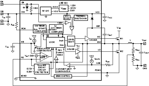
8.2 Functional Block Diagram

8.3 Feature Description
8.3.1 Programming the Output Voltage
The output voltage is set by two external resistors (RFB1,RFB2). The regulated output voltage is calculated as follows:

where
- RFB2 is the top resistor connected between VOUT and FB
- RFB1 is the bottom resistor connected between FB and GND
8.3.2 Regulation Comparator
The feedback voltage at FB is compared to the internal reference voltage of 0.6 V. In normal operation (the output voltage is regulated), an on-time period is initiated when the voltage at FB falls below 0.6 V. The high-side switch stays on for the on-time, causing the FB voltage to rise above 0.6 V. After the on-time period, the high-side switch stays off until the FB voltage falls below 0.6 V.
8.3.3 Overvoltage Comparator
The overvoltage comparator is provided to protect the output from overvoltage conditions due to sudden input line voltage changes or output loading changes. The overvoltage comparator continuously monitors the voltage at the FB pin and compares it to a 0.72 V internal reference. If the voltage at FB rises above 0.72 V, the on-time pulse is immediately terminated. This condition can occur if the input or the output load changes suddenly. Once the overvoltage protection is activated, the HG and LG signals remain off until the voltage at FB pin falls below 0.72 V.
8.3.4 Current Limit
Current limit detection occurs during the off-time by monitoring the current through the low-side switch using an external resistor, RLIM. If during the off-time the current in the low-side switch exceeds the user defined current limit value, the next on-time cycle is immediately terminated. Current sensing is achieved by comparing the voltage across the low side FET with the voltage across the current limit set resistor RLIM. If the voltage across RLIM and the voltage across the low-side FET are equal then the current limit comparator will terminate the next on-time cycle.
The RLIM value can be approximated as follows:


where
- IOCL is the user-defined average output current limit value
- RDS(ON)max is the resistance value of the low-side FET at the expected maximum FET junction temperature
- ILIM-TH is an internal current supply of 85 µA typical
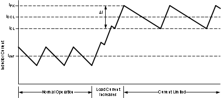
Figure 13 illustrates the inductor current waveform. During normal operation, the output current ripple is dictated by the switching of the FETs. The current through the low-side switch, Ivalley, is sampled at the end of each switching cycle and compared to the current limit, ICL, current. The valley current can be calculated as follows:

where
- IOUT is the average output current
- ΔIL is the peak-to-peak inductor ripple current
If an overload condition occurs, the current through the low-side switch will increase which will cause the current limit comparator to trigger the logic to skip the next on-time cycle. The IC will then try to recover by checking the valley current during each off-time. If the valley current is greater than or equal to ICL, then the IC will keep the low-side FET on and allow the inductor current to further decay.
Throughout the whole process, regardless of the load current, the on-time of the controller will stay constant and thereby the positive ripple current slope will remain constant. During each on-time the current ramps-up an amount equal to:

The valley current limit feature prevents current runaway conditions due to propagation delays or inductor saturation because the inductor current is forced to decay following any overload conditions.
Current sensing is achieved by either a low value sense resistor in series with the low-side FET or by utilizing the RDS(ON) of the low-side FET. The RDS(ON) sensing method is the preferred choice for a more simplified design and lower costs. The RDS(ON) value of a FET has a positive temperature coefficient and will increase in value as the temperature of the FET increases. The LM3150 controller will maintain a more stable current limit that is closer to the original value that was set by the user, by positively adjusting the ILIM-TH value as the IC temperature increases. This does not provide an exact temperature compensation but allows for a more tightly controlled current limit when compared to traditional RDS(ON) sensing methods when the RDS(ON) value can change typically 140% from room to maximum temperature and cause other components to be over-designed. The temperature compensated ILIM-TH is shown below where TJ is the die temperature of the LM3150 controller in Celsius:
To calculate the RLIM value with temperature compensation, substitute Equation 10 into ILIM-TH in Equation 7.
 Figure 13. Inductor Current - Current Limit Operation
8.3.5 Short-Circuit Protection
The LM3150 controller will sense a short-circuit on the output by monitoring the output voltage. When the feedback voltage has fallen below 60% of the reference voltage, Vref x 0.6 (≈ 0.36 V), short-circuit mode of operation will start. During short-circuit operation, the SS pin is discharged and the output voltage will fall to 0 V. The SS pin voltage, VSS, is then ramped back up at the rate determined by the SS capacitor and ISS until VSS reaches 0.7 V. During this re-ramp phase, if the short-circuit fault is still present the output current will be equal to the set current limit. Once the soft-start voltage reaches 0.7 V, the output voltage is sensed again and if the VFB is still below Vref x 0.6 then the SS pin is discharged again and the cycle repeats until the short-circuit fault is removed.
8.3.6 Soft-Start
The soft-start (SS) feature allows the regulator to gradually reach a steady-state operating point, which reduces start-up stresses and current surges. At turnon, while VCC is below the undervoltage threshold, the SS pin is internally grounded and VOUT is held at 0 V. The SS capacitor is used to slowly ramp VFB from 0 V to 0.6 V. By changing the capacitor value, the duration of start-up can be changed accordingly. The start-up time can be calculated using the following equation:

where
- tSS is measured in seconds
- Vref = 0.6 V
- ISS is the soft-start pin source current, which is typically 7.7 µA (refer to Electrical Characteristics)
An internal switch grounds the SS pin if VCC is below the undervoltage lockout threshold, if a thermal shutdown occurs, or if the EN pin is grounded. By using an externally controlled switch, the output voltage can be shut off by grounding the SS pin.
During startup the LM3150 controller will operate in diode emulation mode, where the low-side gate LG will turn off and remain off when the inductor current falls to zero. Diode emulation mode will allow start-up into a pre-biased output voltage. When soft-start is greater than 0.7 V, the LM3150 controller will remain in continuous conduction mode. During diode emulation mode at current limit the low-gate will remain off when the inductor current is off.
The soft-start time should be greater than the input voltage rise time and also satisfy the following equality to maintain a smooth transition of the output voltage to the programmed regulation voltage during start-up.
8.3.7 Thermal Protection
The LM3150 controller should be operated such that the junction temperature does not exceed the maximum operating junction temperature. An internal thermal shutdown circuit, which activates at 165°C (typical), takes the controller to a low-power reset state by disabling the buck switch and the on-timer, and grounding the SS pin. This feature helps prevent catastrophic failures from accidental device overheating. When the junction temperature falls back below 150°C the SS pin is released and device operation resumes.
8.4 Device Functional Modes
The EN pin can be activated by either leaving the pin floating due to an internal pullup resistor to VIN or by applying a logic high signal to the EN pin of 1.26 V or greater. The LM3150 controller can be remotely shut down by taking the EN pin below 1.02 V. Low quiescent shutdown is achieved when VEN is less than 0.4 V. During low quiescent shutdown the internal bias circuitry is turned off.
The LM3150 controller has certain fault conditions that can trigger shutdown, such as short circuit, undervoltage lockout, or thermal shutdown. During shutdown, the soft-start capacitor is discharged. Once the fault condition is removed, the soft-start capacitor begins charging, allowing the part to start-up in a controlled fashion. In conditions where there may be an open drain connection to the EN pin, it may be necessary to add a 1-nF bypass capacitor to this pin. This will help decouple noise from the EN pin and prevent false disabling.