SNVSAY0 June 2017 LM317-N-MIL
PRODUCTION DATA.
- 1 Features
- 2 Applications
- 3 Description
- 4 Revision History
- 5 Pin Configuration and Functions
- 6 Specifications
- 7 Detailed Description
-
8 Application and Implementation
- 8.1 Application Information
- 8.2
Typical Applications
- 8.2.1 1.25-V to 25-V Adjustable Regulator
- 8.2.2 5-V Logic Regulator With Electronic Shutdown
- 8.2.3 Slow Turnon 15-V Regulator
- 8.2.4 Adjustable Regulator With Improved Ripple Rejection
- 8.2.5 High Stability 10-V Regulator
- 8.2.6 High-Current Adjustable Regulator
- 8.2.7 Emitter-Follower Current Amplifier
- 8.2.8 1-A Current Regulator
- 8.2.9 Common-Emitter Amplifier
- 8.2.10 Low-Cost 3-A Switching Regulator
- 8.2.11 Current-Limited Voltage Regulator
- 8.2.12 Adjusting Multiple On-Card Regulators With Single Control
- 8.2.13 AC Voltage Regulator
- 8.2.14 12-V Battery Charger
- 8.2.15 Adjustable 4-A Regulator
- 8.2.16 Current-Limited 6-V Charger
- 8.2.17 Digitally Selected Outputs
- 9 Power Supply Recommendations
- 10Layout
- 11Device and Documentation Support
- 12Mechanical, Packaging, and Orderable Information
Package Options
Mechanical Data (Package|Pins)
- NDS|2
Thermal pad, mechanical data (Package|Pins)
Orderable Information
10 Layout
10.1 Layout Guidelines
Some layout guidelines must be followed to ensure proper regulation of the output voltage with minimum noise. Traces carrying the load current must be wide to reduce the amount of parasitic trace inductance and the feedback loop from VOUT to ADJ must be kept as short as possible. To improve PSRR, a bypass capacitor can be placed at the ADJ pin and must be located as close as possible to the IC. In cases when VIN shorts to ground, an external diode must be placed from VOUT to VIN to divert the surge current from the output capacitor and protect the IC. Similarly, in cases when a large bypass capacitor is placed at the ADJ pin and VOUT shorts to ground, an external diode must be placed from ADJ to VOUT to provide a path for the bypass capacitor to discharge. These diodes must be placed close to the corresponding IC pins to increase their effectiveness.
10.2 Layout Example
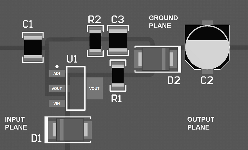 Figure 36. Layout Example (SOT-223)
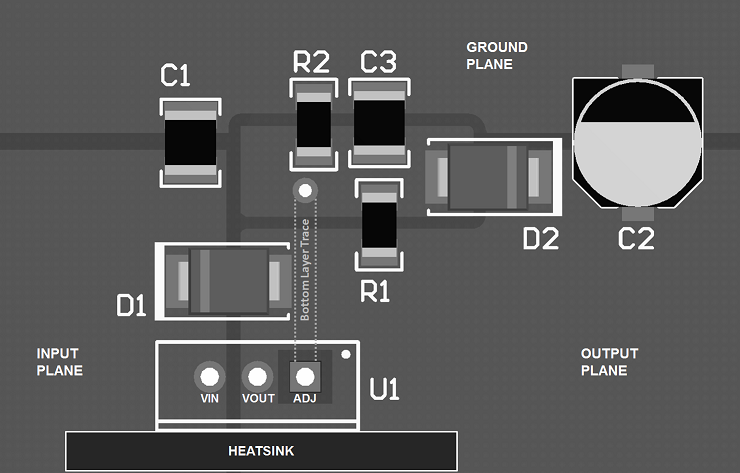 Figure 37. Layout Example (TO-220)
10.3 Thermal Considerations
10.3.1 Heatsink Requirements
The LM317-N-MIL regulators have internal thermal shutdown to protect the device from over-heating. Under all operating conditions, the junction temperature of the LM317-N-MIL must not exceed the rated maximum junction temperature (TJ) of 125°C. A heatsink may be required depending on the maximum device power dissipation and the maximum ambient temperature of the application. To determine if a heatsink is needed, the power dissipated by the regulator, PD, must be calculate with Equation 3:
Figure 38 shows the voltage and currents which are present in the circuit.
The next parameter which must be calculated is the maximum allowable temperature rise, TR(MAX) in Equation 4:
where TJ(MAX) is the maximum allowable junction temperature (125°C for the LM317-N-MIL), and TA(MAX) is the maximum ambient temperature that will be encountered in the application.
Using the calculated values for TR(MAX) and PD, the maximum allowable value for the junction-to-ambient thermal resistance (θJA) can be calculated with Equation 5:
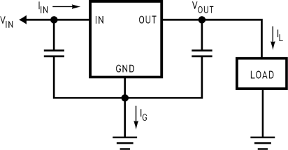 Figure 38. Power Dissipation Diagram
If the calculated maximum allowable thermal resistance is higher than the actual package rating, then no additional work is needed. If the calculated maximum allowable thermal resistance is lower than the actual package rating either the power dissipation (PD) needs to be reduced, the maximum ambient temperature TA(MAX) needs to be reduced, the thermal resistance (θJA) must be lowered by adding a heatsink, or some combination of these.
If a heatsink is needed, the value can be calculated from Equation 6:
where
- θCH is the thermal resistance of the contact area between the device case and the heatsink surface
- θJC is thermal resistance from the junction of the die to surface of the package case
When a value for θHA is found using the equation shown, a heatsink must be selected that has a value that is less than, or equal to, this number.
The θHA rating is specified numerically by the heatsink manufacturer in the catalog, or shown in a curve that plots temperature rise vs power dissipation for the heatsink.
10.3.2 Heatsinking Surface Mount Packages
The TO-263 (KTT), SOT-223 (DCY) and TO-252 (NDP) packages use a copper plane on the PCB and the PCB itself as a heatsink. To optimize the heat sinking ability of the plane and PCB, solder the tab of the package to the plane.
10.3.2.1 Heatsinking the SOT-223 (DCY) Package
Figure 39 and Figure 40 show the information for the SOT-223 package. Figure 40 assumes a θJA of 74°C/W for 1-oz. copper and 59.6°C/W for 2-oz. copper and a maximum junction temperature of 125°C. See AN-1028 (SNVA036) for thermal enhancement techniques to be used with SOT-223 and TO-252 packages.
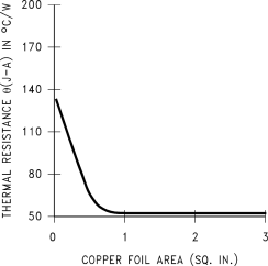 Figure 39. θJA vs Copper (2-oz.) Area for the SOT-223 Package
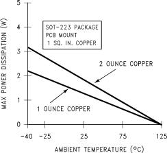 Figure 40. Maximum Power Dissipation vs TAMB for the SOT-223 Package
10.3.2.2 Heatsinking the TO-263 (KTT) Package
Figure 41 shows for the TO-263 the measured values of θJA for different copper area sizes using a typical PCB with 1-oz. copper and no solder mask over the copper area used for heatsinking.
As shown in Figure 41, increasing the copper area beyond 1 square inch produces very little improvement. It must also be observed that the minimum value of θJA for the TO-263 package mounted to a PCB is 32°C/W.
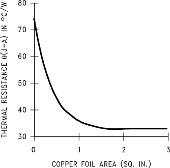 Figure 41. θJA vs Copper (1-oz.) Area for the TO-263 Package
As a design aid, Figure 42 shows the maximum allowable power dissipation compared to ambient temperature for the TO-263 device (assuming θJA is 35°C/W and the maximum junction temperature is 125°C).
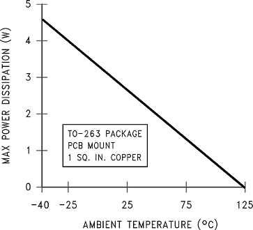 Figure 42. Maximum Power Dissipation vs TAMB for the TO-263 Package
10.3.2.3 Heatsinking the TO-252 (NDP) Package
If the maximum allowable value for θJA is found to be ≥ 54°C/W (typical rated value) for the TO-252 package, no heatsink is needed because the package alone will dissipate enough heat to satisfy these requirements. If the calculated value for θJA falls below these limits, a heatsink is required.
As a design aid, Table 1 shows the value of the θJA of NDP the package for different heatsink area. The copper patterns that we used to measure these θJAs are shown in Figure 47. Figure 43 reflects the same test results as what are in Table 1.
Figure 44 shows the maximum allowable power dissipation versus ambient temperature for the TO-252 device. Figure 45 shows the maximum allowable power dissipation versus copper area (in2) for the TO-252 device. See AN-1028 (SNVA036) for thermal enhancement techniques to be used with SOT-223 and TO-252 packages.
Table 1. θJA Different Heatsink Area
| LAYOUT | COPPER AREA | THERMAL RESISTANCE | |
|---|---|---|---|
| Top Side (in2)(1) | Bottom Side (in2) | (θJA°C/W) TO-252 | |
| 1 | 0.0123 | 0 | 103 |
| 2 | 0.066 | 0 | 87 |
| 3 | 0.3 | 0 | 60 |
| 4 | 0.53 | 0 | 54 |
| 5 | 0.76 | 0 | 52 |
| 6 | 1.0 | 0 | 47 |
| 7 | 0.066 | 0.2 | 84 |
| 8 | 0.066 | 0.4 | 70 |
| 9 | 0.066 | 0.6 | 63 |
| 10 | 0.066 | 0.8 | 57 |
| 11 | 0.066 | 1.0 | 57 |
| 12 | 0.066 | 0.066 | 89 |
| 13 | 0.175 | 0.175 | 72 |
| 14 | 0.284 | 0.284 | 61 |
| 15 | 0.392 | 0.392 | 55 |
| 16 | 0.5 | 0.5 | 53 |
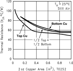 Figure 43. θJA vs 2-oz. Copper Area for TO-252
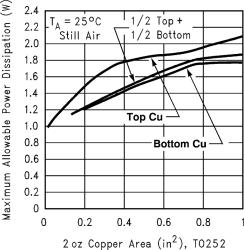 Figure 45. Maximum Allowable Power Dissipation vs 2-oz. Copper Area for TO-252
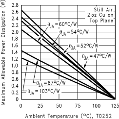 Figure 44. Maximum Allowable Power Dissipation vs Ambient Temperature for TO-252
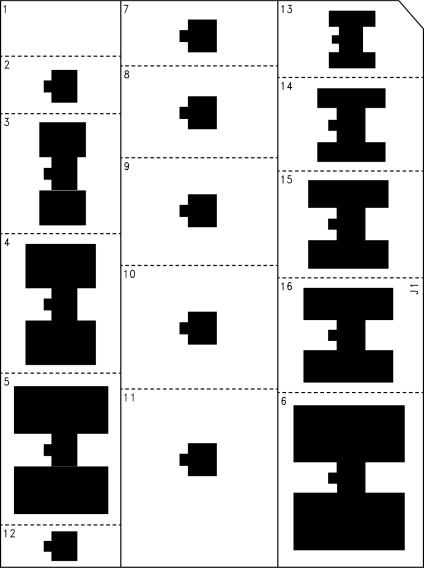 Figure 46. Top View of the Thermal Test Pattern in Actual Scale
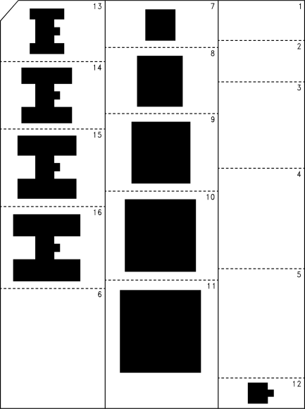 Figure 47. Bottom View of the Thermal Test Pattern in Actual Scale