SNOSC16D March 2000 – January 2015 LM124-N , LM224-N , LM2902-N , LM324-N
PRODUCTION DATA.
- 1 Features
- 2 Applications
- 3 Description
- 4 Revision History
- 5 Pin Configuration and Functions
- 6 Specifications
- 7 Detailed Description
- 8 Application and Implementation
- 9 Power Supply Recommendations
- 10Layout
- 11Device and Documentation Support
- 12Mechanical, Packaging, and Orderable Information
Package Options
Mechanical Data (Package|Pins)
Thermal pad, mechanical data (Package|Pins)
Orderable Information
8 Application and Implementation
NOTE
Information in the following applications sections is not part of the TI component specification, and TI does not warrant its accuracy or completeness. TI’s customers are responsible for determining suitability of components for their purposes. Customers should validate and test their design implementation to confirm system functionality.
8.1 Application Information
The LM124 series of amplifiers is specified for operation from 3 V to 32 V (±1.5 V to ±16 V). Many of the specifications apply from –40°C to 125°C. Parameters that can exhibit significant variance with regards to operating voltage or temperature are presented in Typical Characteristics.
8.2 Typical Applications
Figure 15 emphasizes operation on only a single power supply voltage. If complementary power supplies are available, all of the standard op amp circuits can be used. In general, introducing a pseudo-ground (a bias voltage reference of V+/2) will allow operation above and below this value in single power supply systems. Many application circuits are shown which take advantage of the wide input common-mode voltage range which includes ground. In most cases, input biasing is not required and input voltages which range to ground can easily be accommodated.
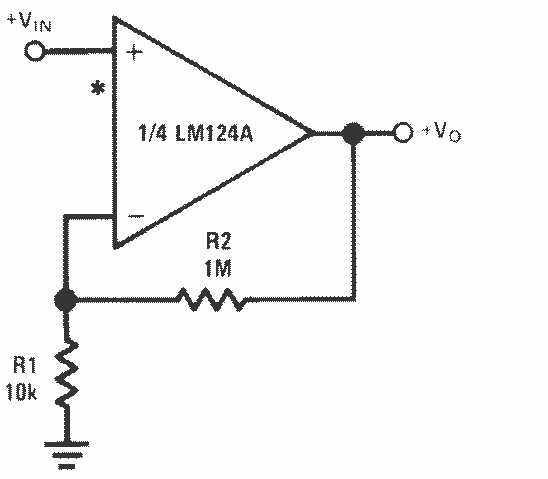
8.2.1 Non-Inverting DC Gain (0 V Input = 0 V Output)
8.2.1.1 Design Requirements
For this example application, the required signal gain is a non-inverting 100x±5% with a supply voltage of 5 V.
8.2.1.2 Detailed Design Procedure
Using the equation for a non-inverting gain configuration, Av = 1+R2/R1. Setting the R1 to 10 kΩ, R2 is 99 times larger than R1, which is 990 kΩ. A 1MΩ is more readily available, and provides a gain of 101, which is within the desired specification.
The gain-frequency characteristic of the amplifier and its feedback network must be such that oscillation does not occur. To meet this condition, the phase shift through amplifier and feedback network must never exceed 180° for any frequency where the gain of the amplifier and its feedback network is greater than unity. In practical applications, the phase shift should not approach 180° since this is the situation of conditional stability. Obviously the most critical case occurs when the attenuation of the feedback network is zero.
8.2.1.3 Application Curve
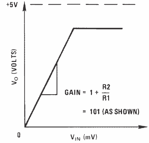 Figure 16. Non-Inverting Amplified Response Curve
8.2.2 Other Application Circuits at V+ = 5.0 VDC
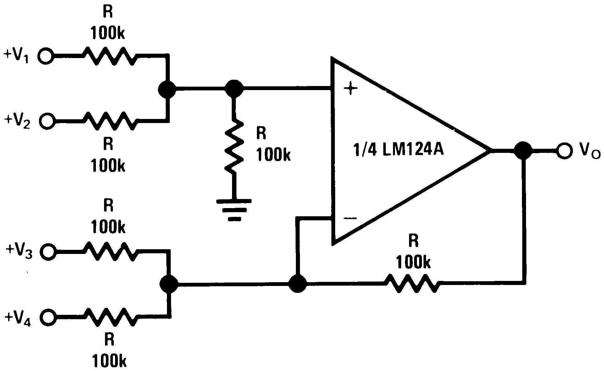
| Where: | V0 = V1 + V2 − V3 − V4 | |
| (V1 + V2) ≥ (V3 + V4) to keep VO > 0 VDC | ||
(VIN'S ≥ 0 VDC And VO ≥ VDC)
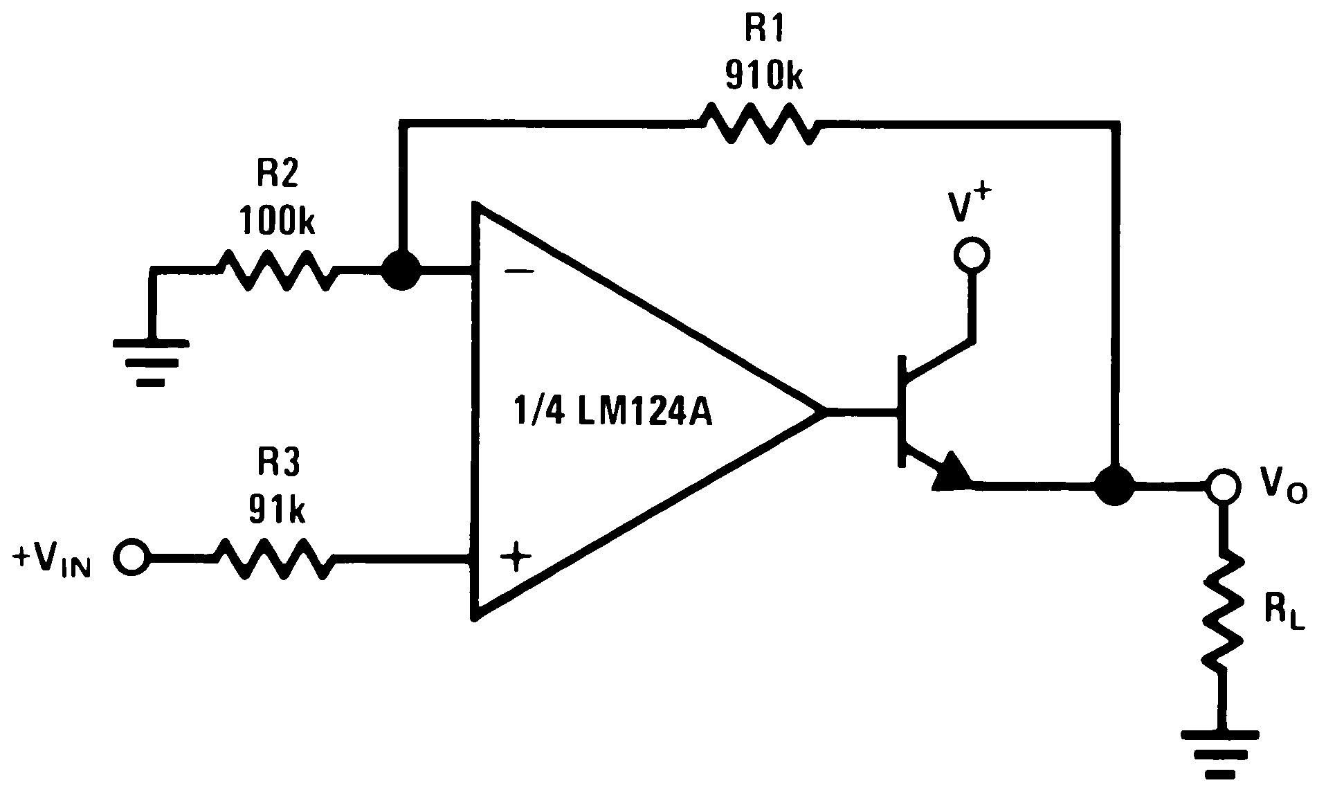
| Where: | V0 = 0 VDC for VIN = 0 VDC | |
| AV = 10 |
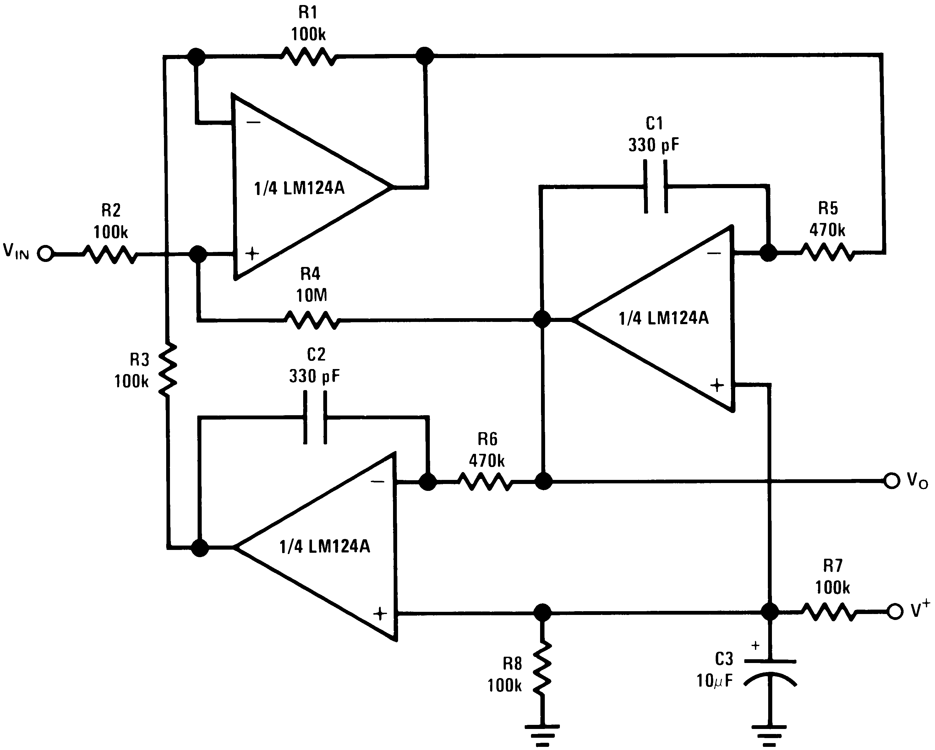
| fo = 1 kHz | Q = 50 | AV = 100 (40 dB) |
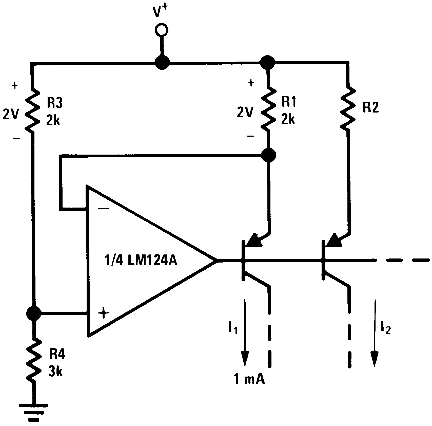
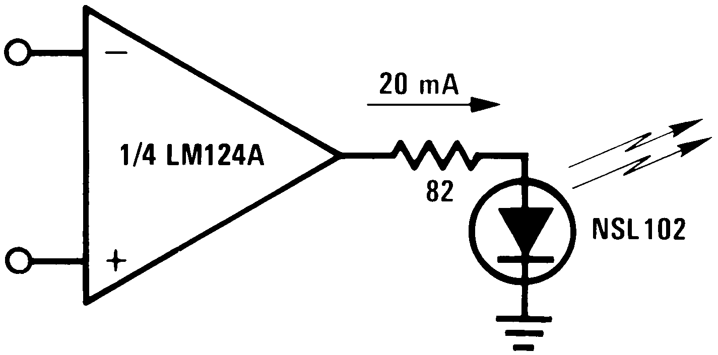
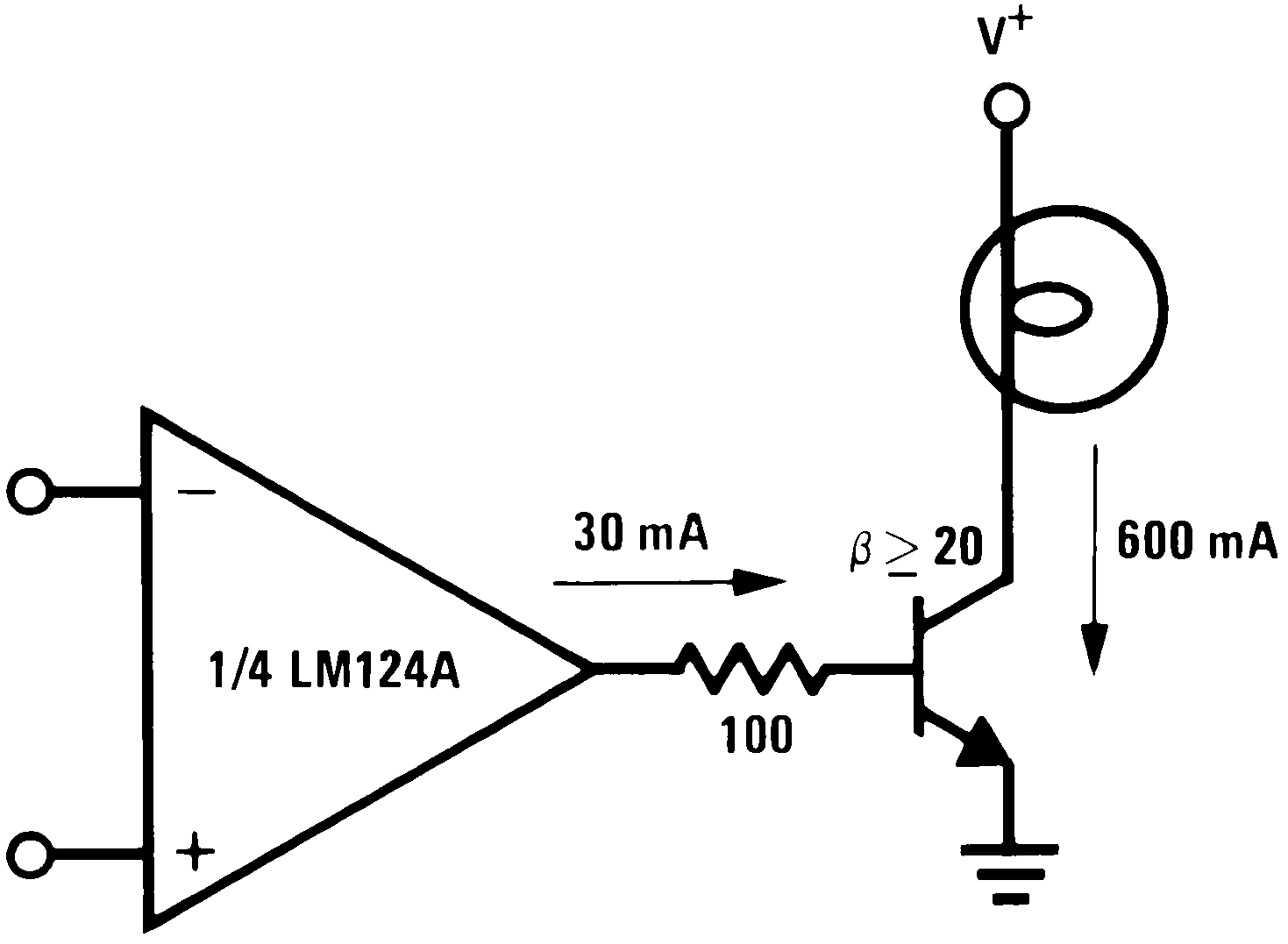 Figure 22. Lamp Driver
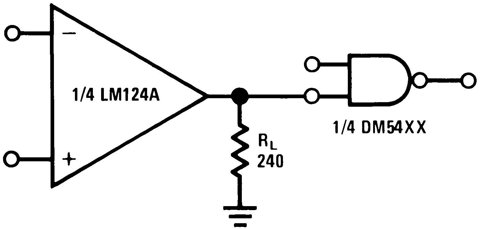 Figure 24. Driving TTL
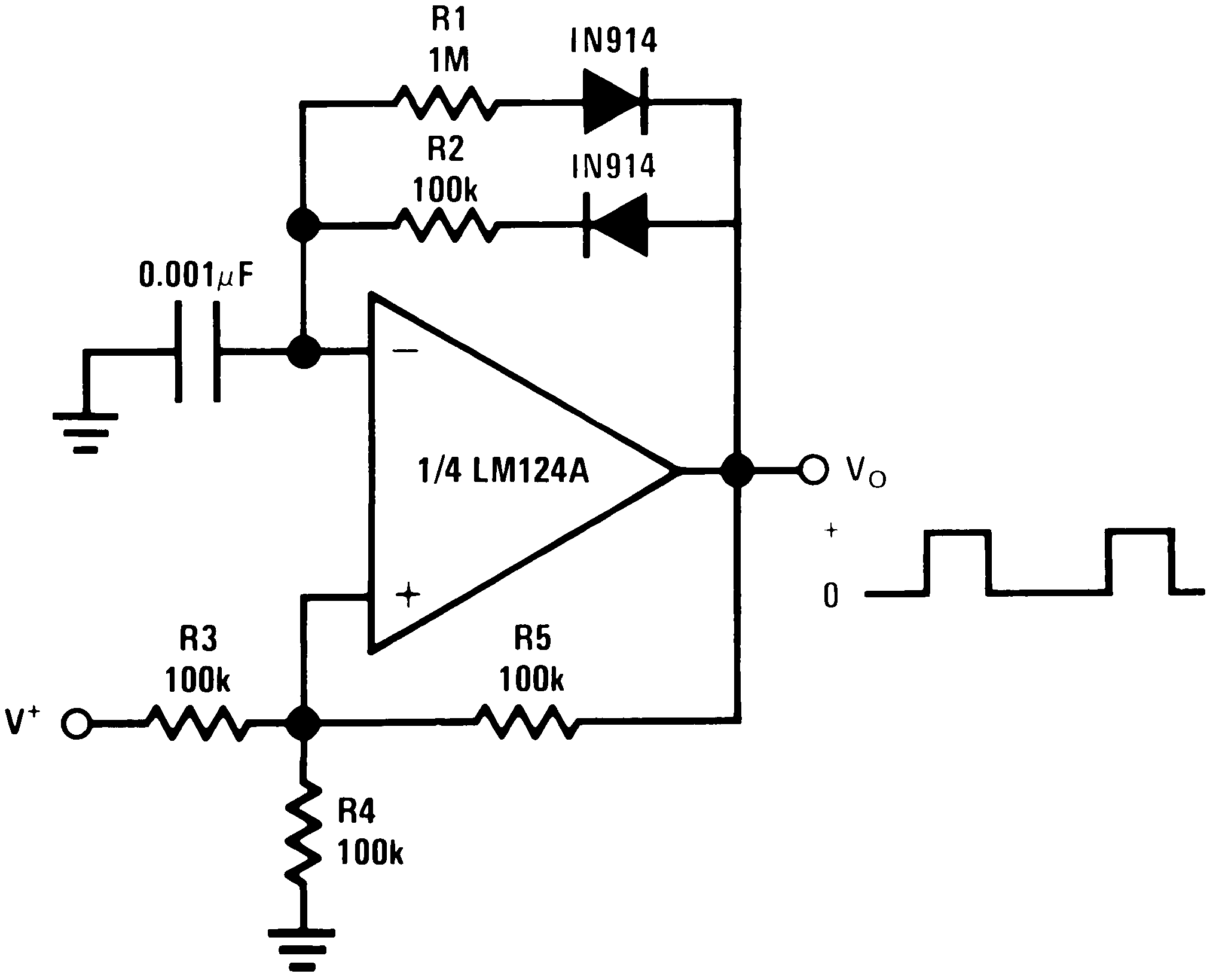 Figure 26. Pulse Generator
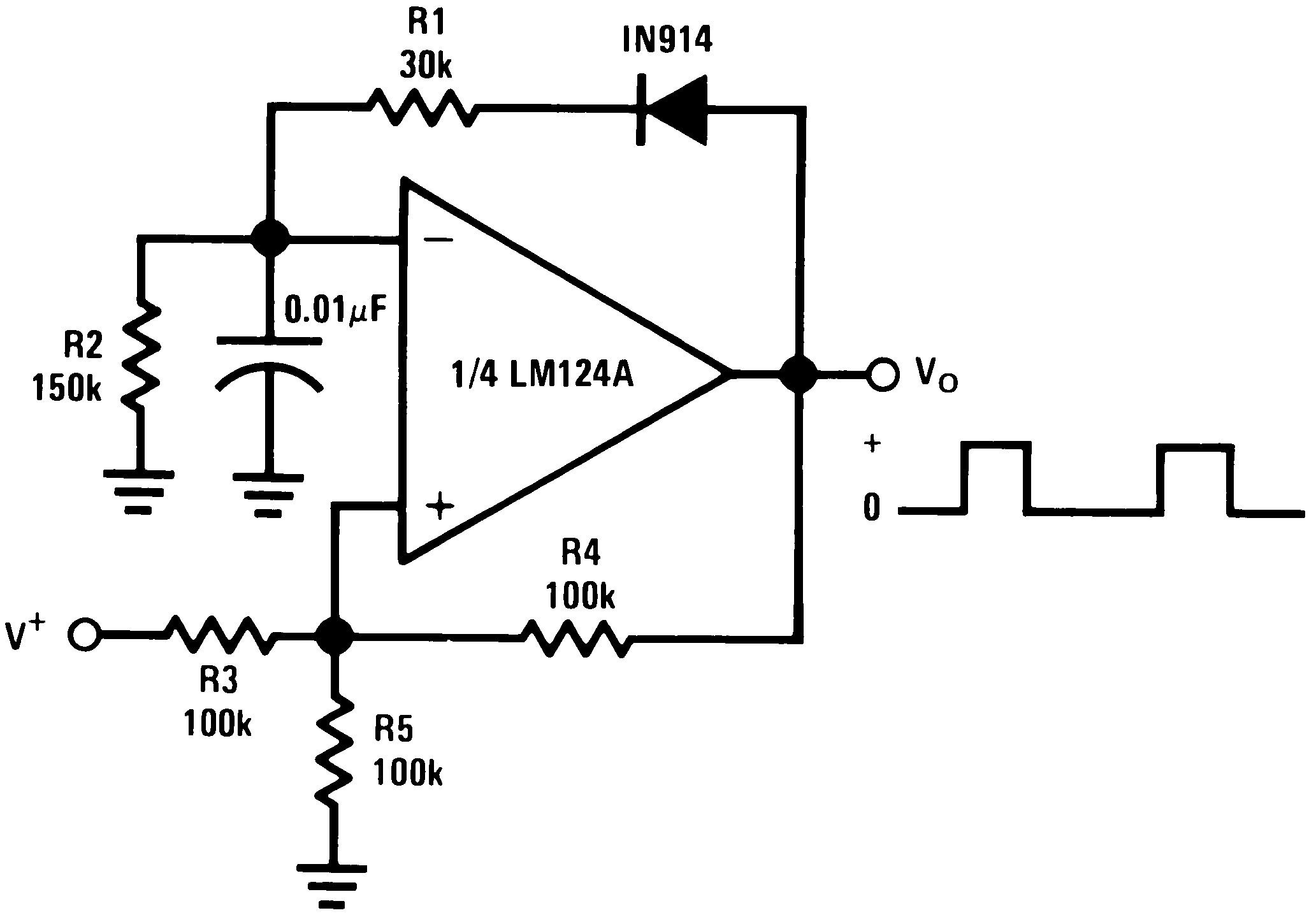 Figure 28. Pulse Generator
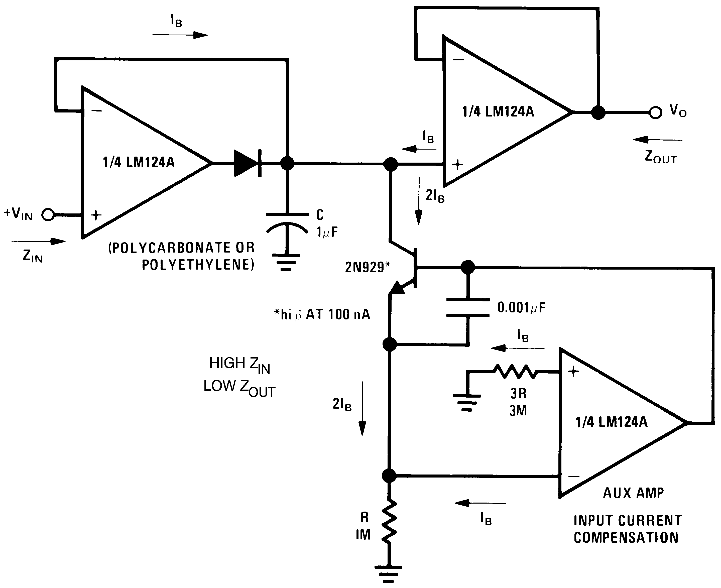 Figure 30. Low Drift Peak Detector
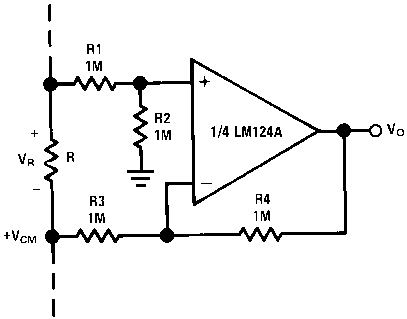
| VO = VR | ||
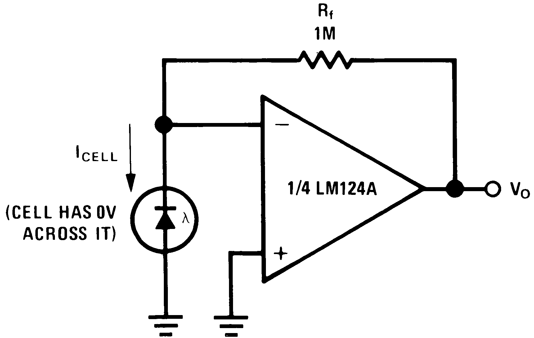
| Q = 1 | AV = 2 | |
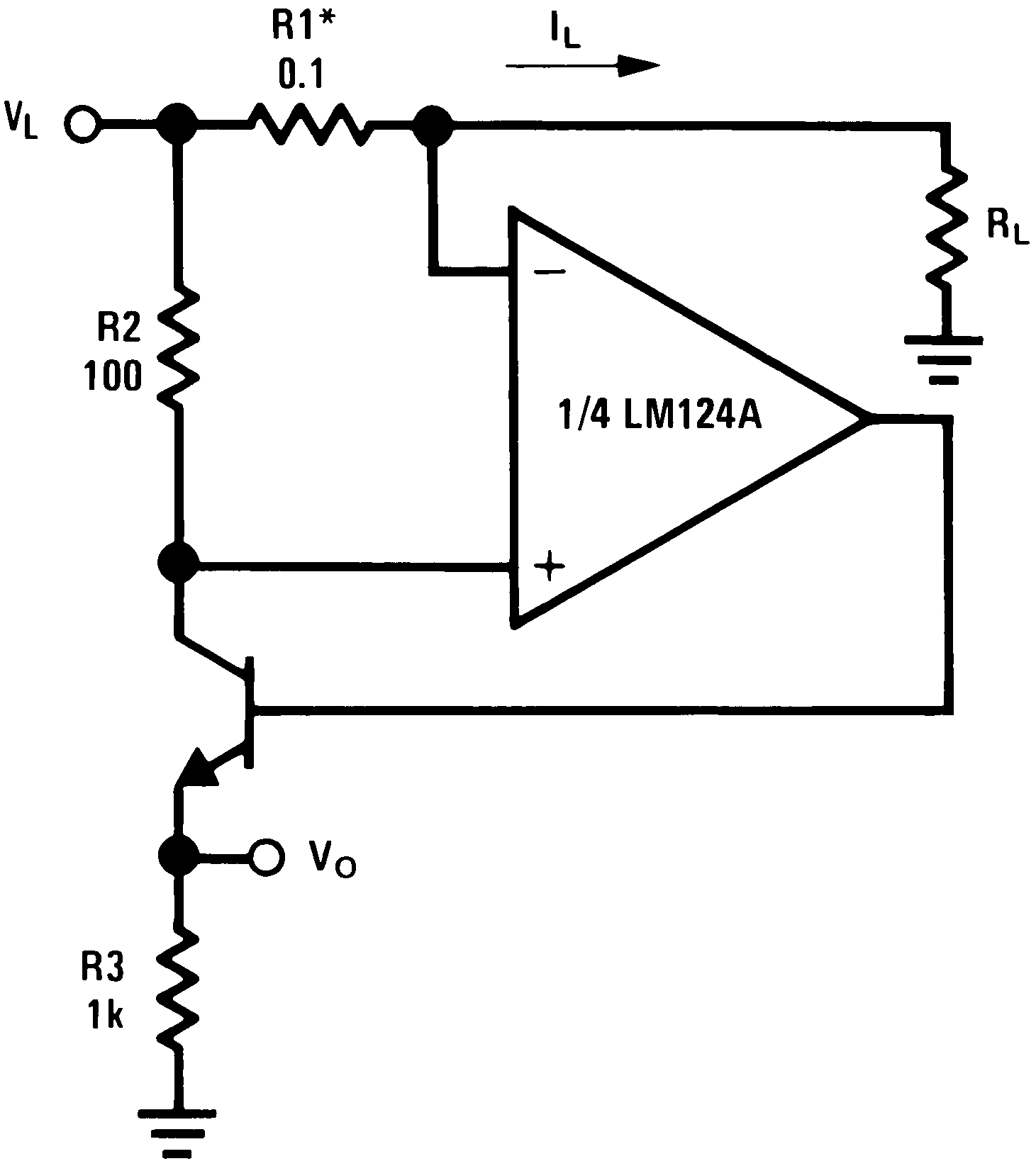
| *(Increase R1 for IL small) | ||
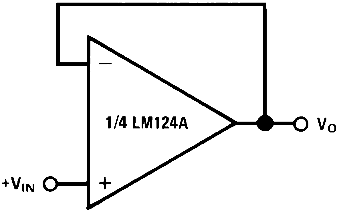 Figure 25. Voltage Follower
 Figure 27. Squarewave Oscillator
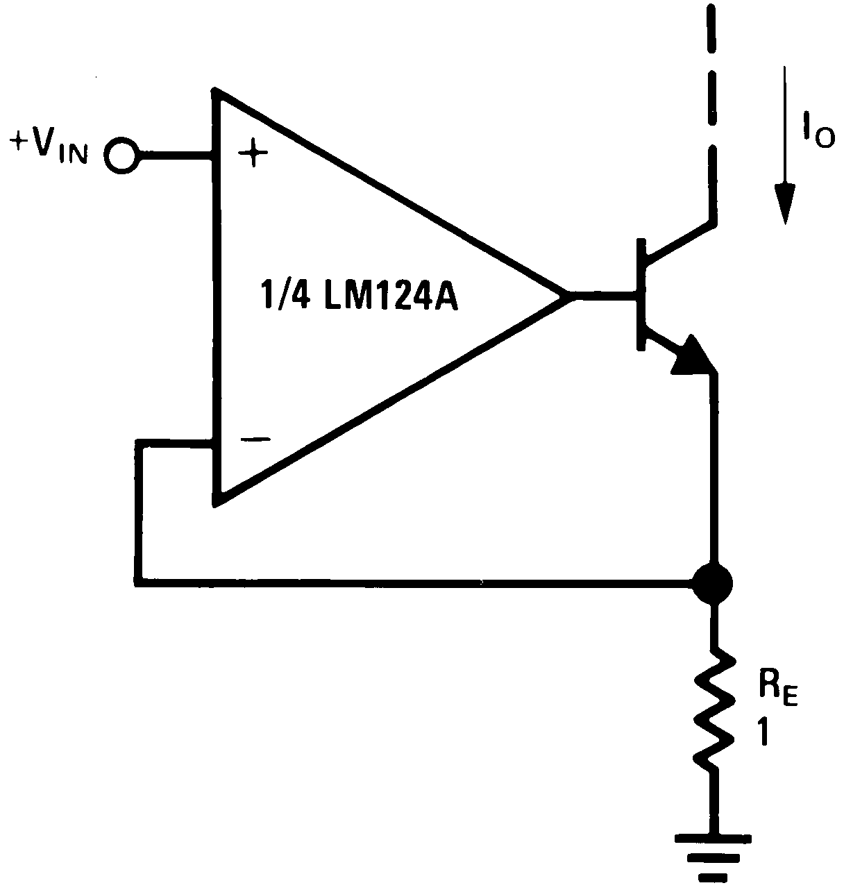
| IO = 1 amp/volt VIN | (Increase RE for Io small) | |
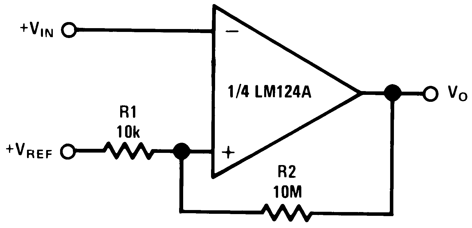 Figure 31. Comparator With Hysteresis
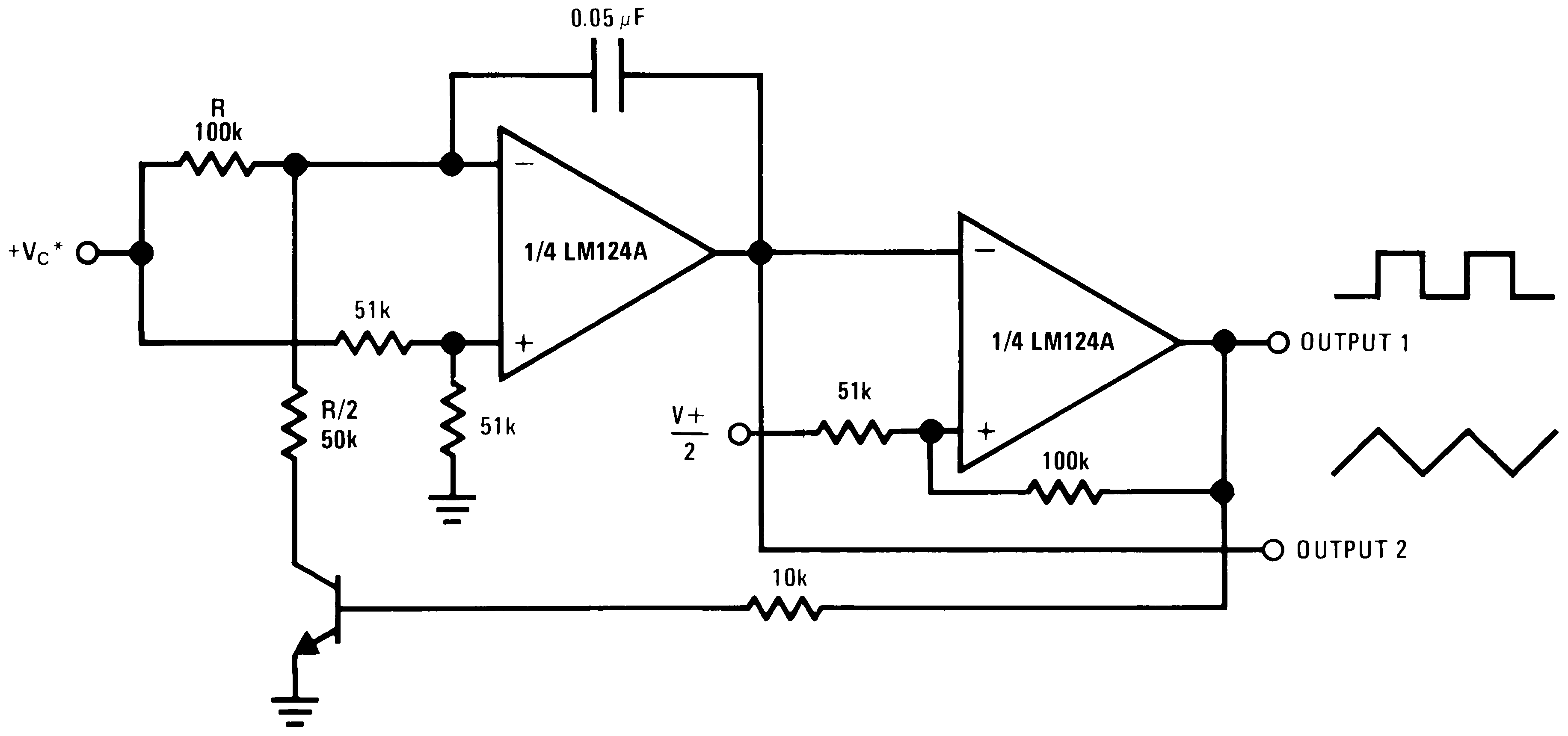
| *Wide control voltage range: 0 VDC ≤ VC ≤ 2 (V+ −1.5 VDC) |
||
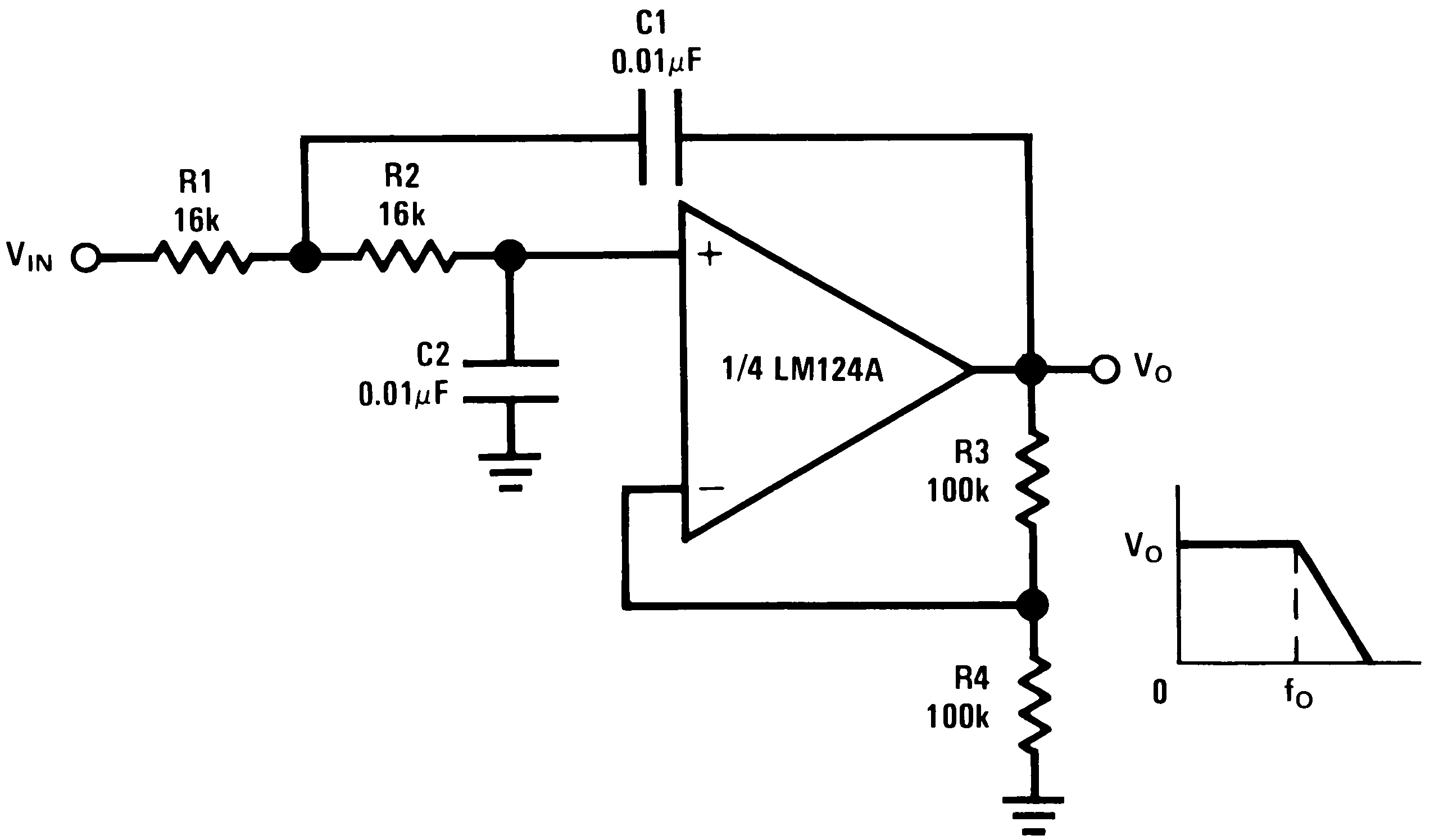
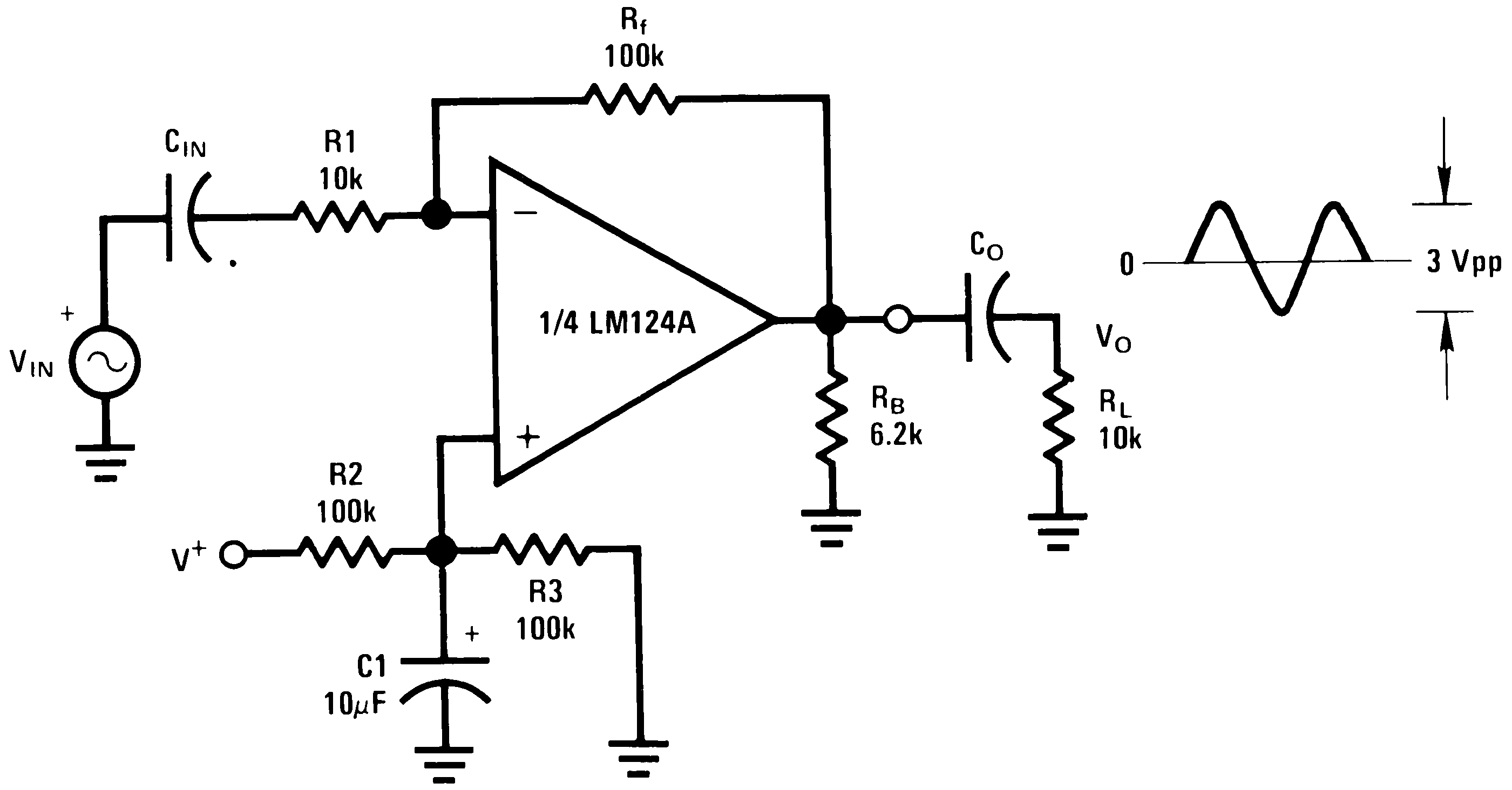
 Figure 36. AC Coupled Inverting Amplifier
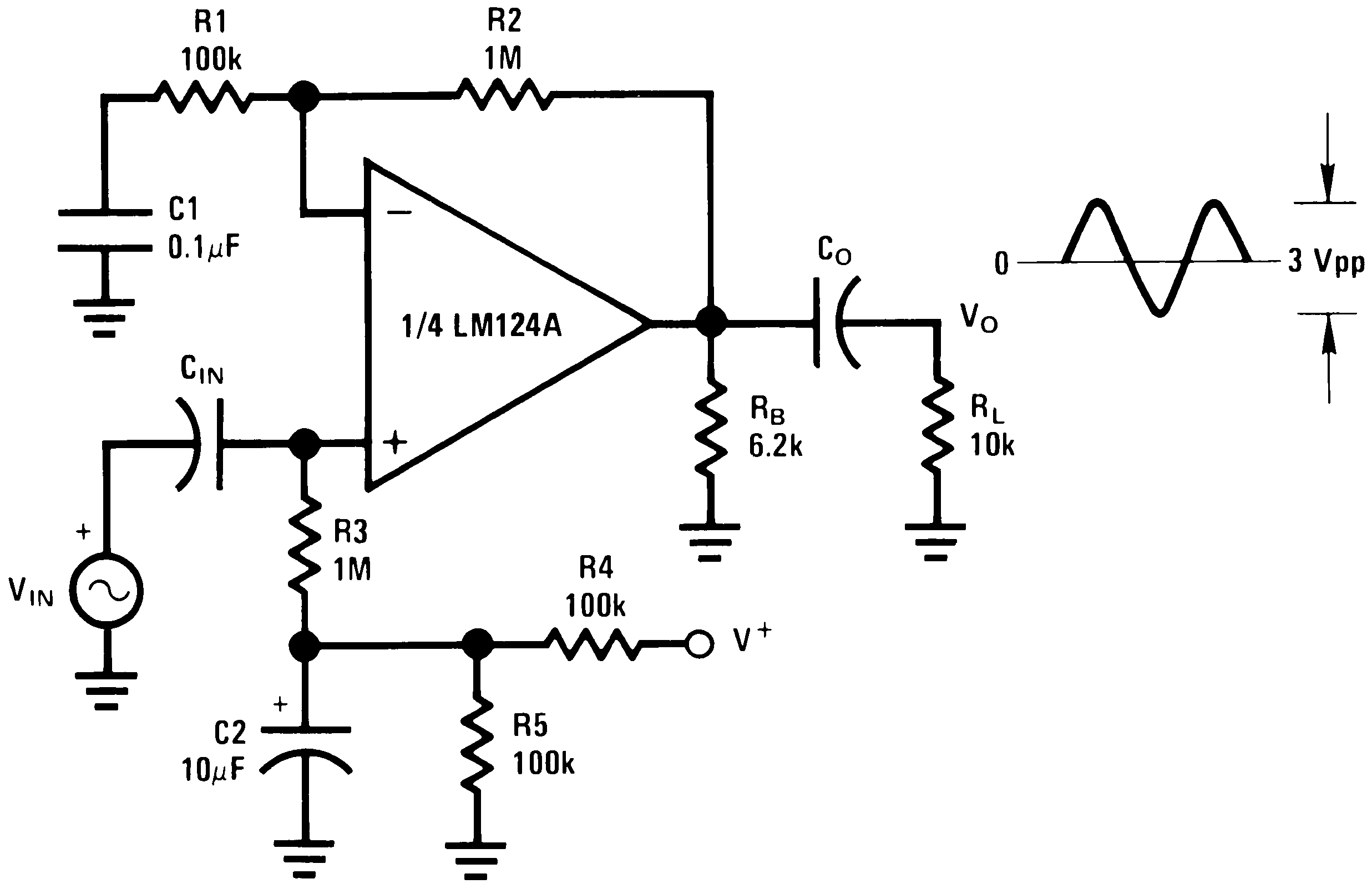
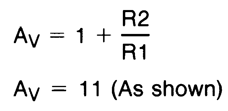 Figure 37. AC Coupled Non-Inverting Amplifier
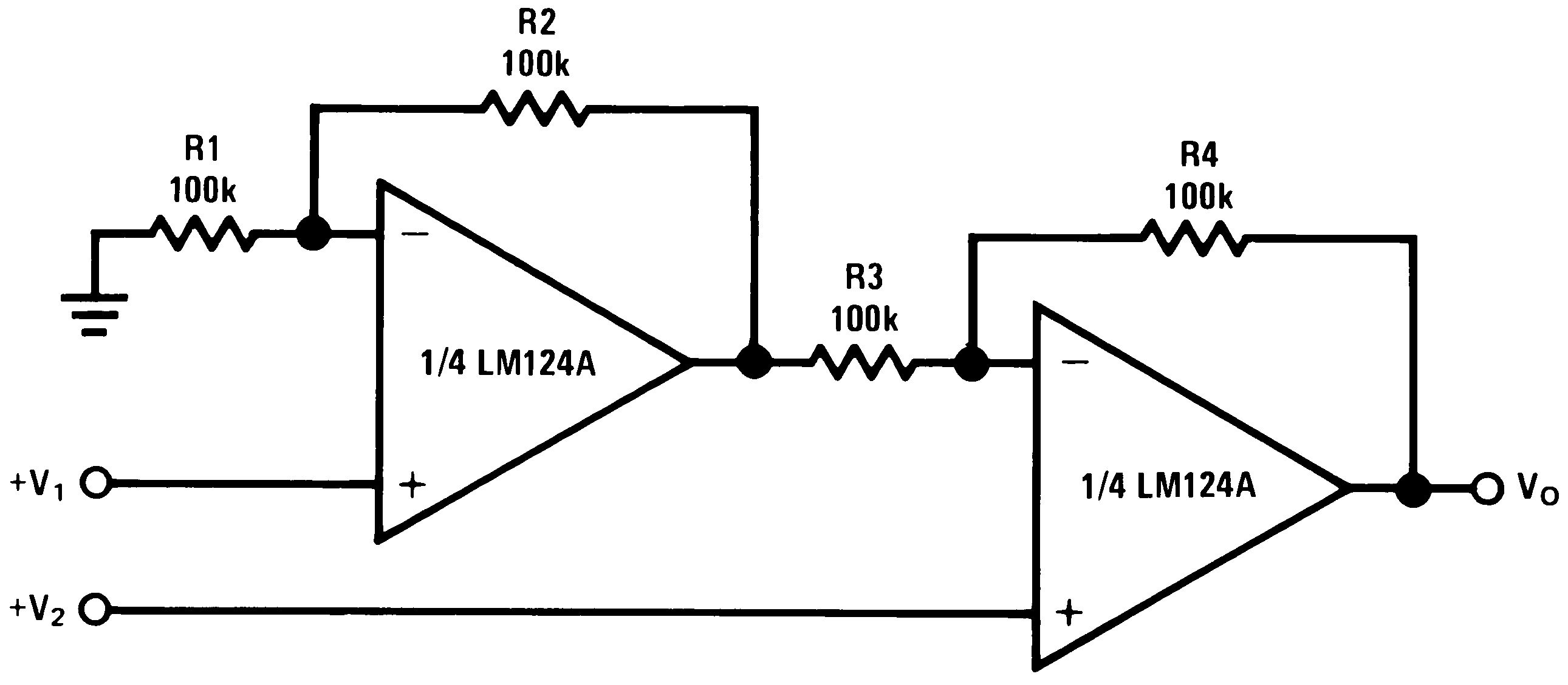
 Figure 38. High Input Z, DC Differential Amplifier
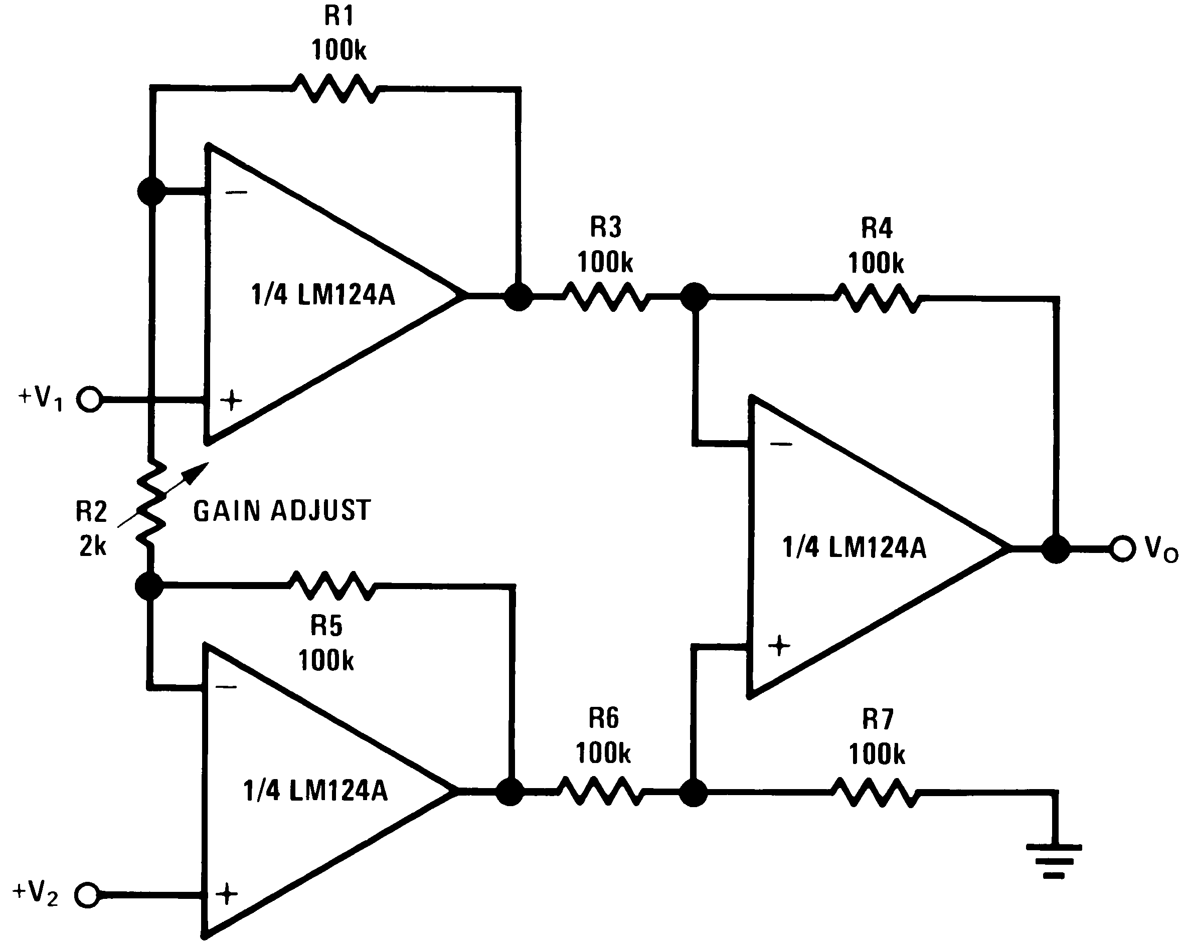
 Figure 39. High Input Z Adjustable-Gain DC Instrumentation Amplifier
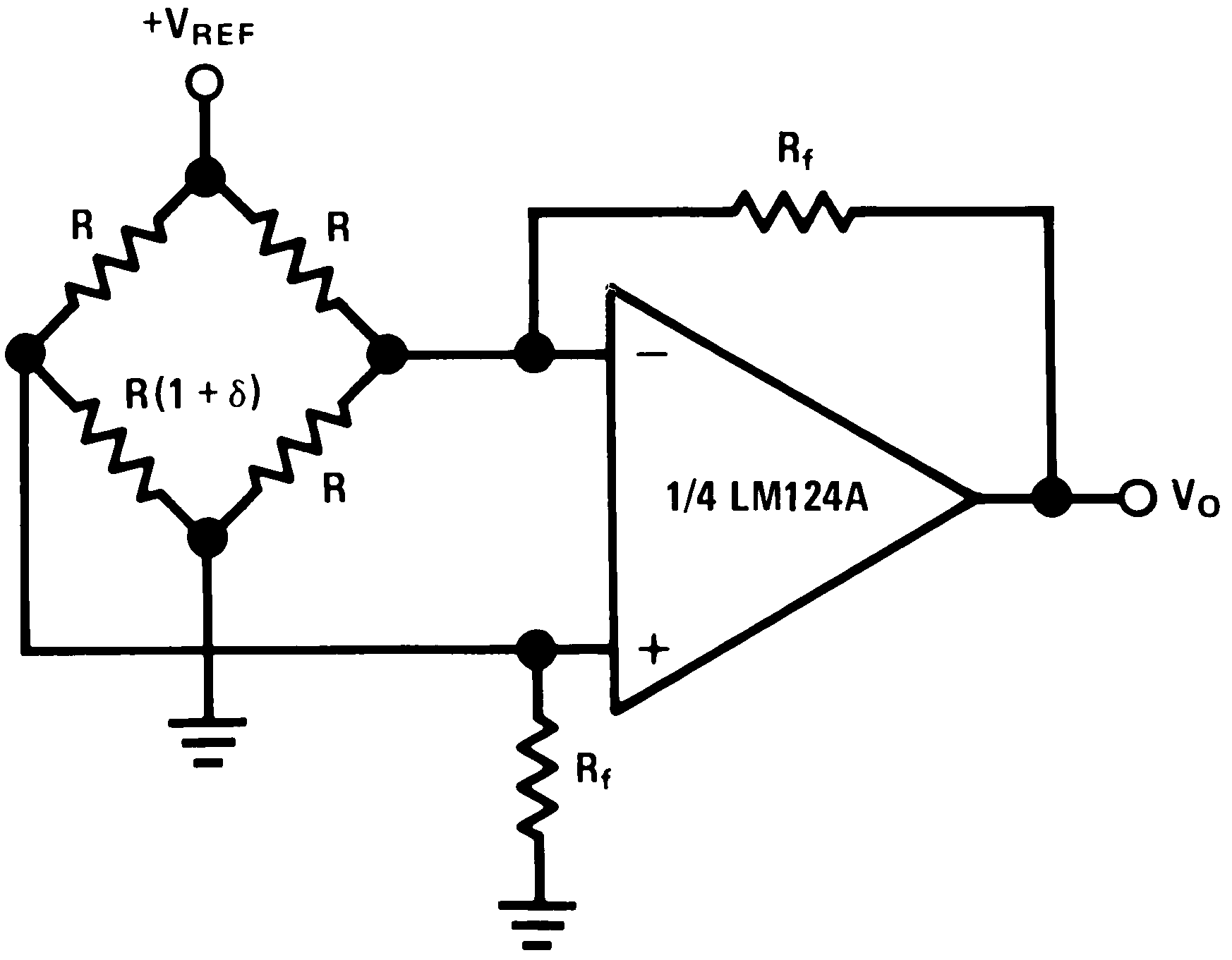
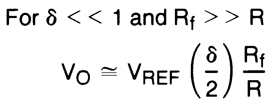 Figure 40. Bridge Current Amplifier
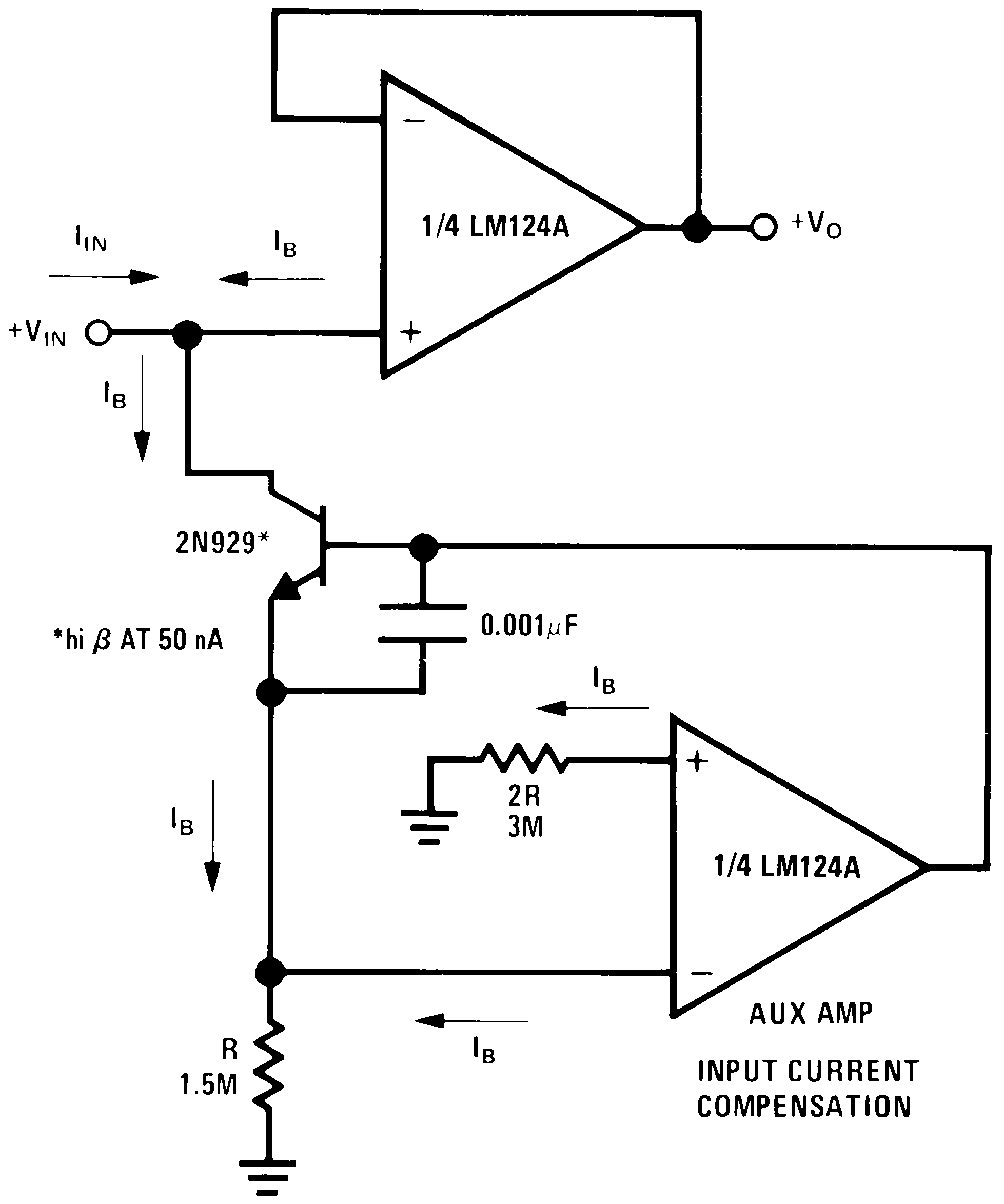 Figure 41. Using Symmetrical Amplifiers to Reduce Input Current (General Concept)
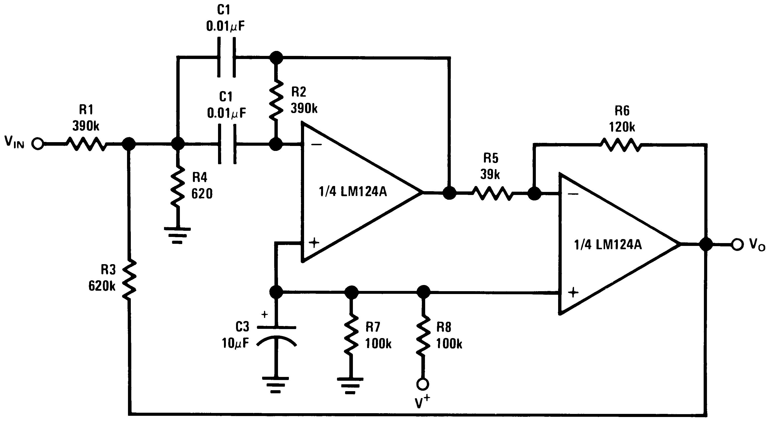
| fO = 1 kHz | Q = 25 | |