SNOSBJ3E November 1999 – December 2014 LM139-N , LM239-N , LM2901-N , LM339-N
PRODUCTION DATA.
- 1 Features
- 2 Applications
- 3 Description
- 4 Revision History
- 5 Pin Configuration and Functions
- 6 Specifications
- 7 Detailed Description
- 8 Application and Implementation
- 9 Power Supply Recommendations
- 10Layout
- 11Device and Documentation Support
- 12Mechanical, Packaging, and Orderable Information
Package Options
Mechanical Data (Package|Pins)
Thermal pad, mechanical data (Package|Pins)
Orderable Information
8 Application and Implementation
NOTE
Information in the following applications sections is not part of the TI component specification, and TI does not warrant its accuracy or completeness. TI’s customers are responsible for determining suitability of components for their purposes. Customers should validate and test their design implementation to confirm system functionality.
8.1 Application Information
The LM139-N is specified for operation from 2.0 V to 36 V (±1V to ±18V) over the temperature range of –55°C to 125°C. While it may seem like a comparator has a well-defined and somewhat limited functionality as a '1-bit ADC', a comparator is a versatile component which can be used for many functions.
Refer to AN-74 LM139/LM239/LM339 A Quad of Independently Functioning Comparators (SNOA654) for additional application information on use of the LM139-N.
8.2 Typical Applications
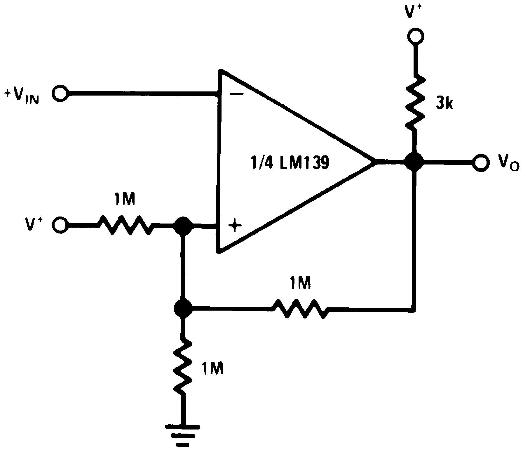
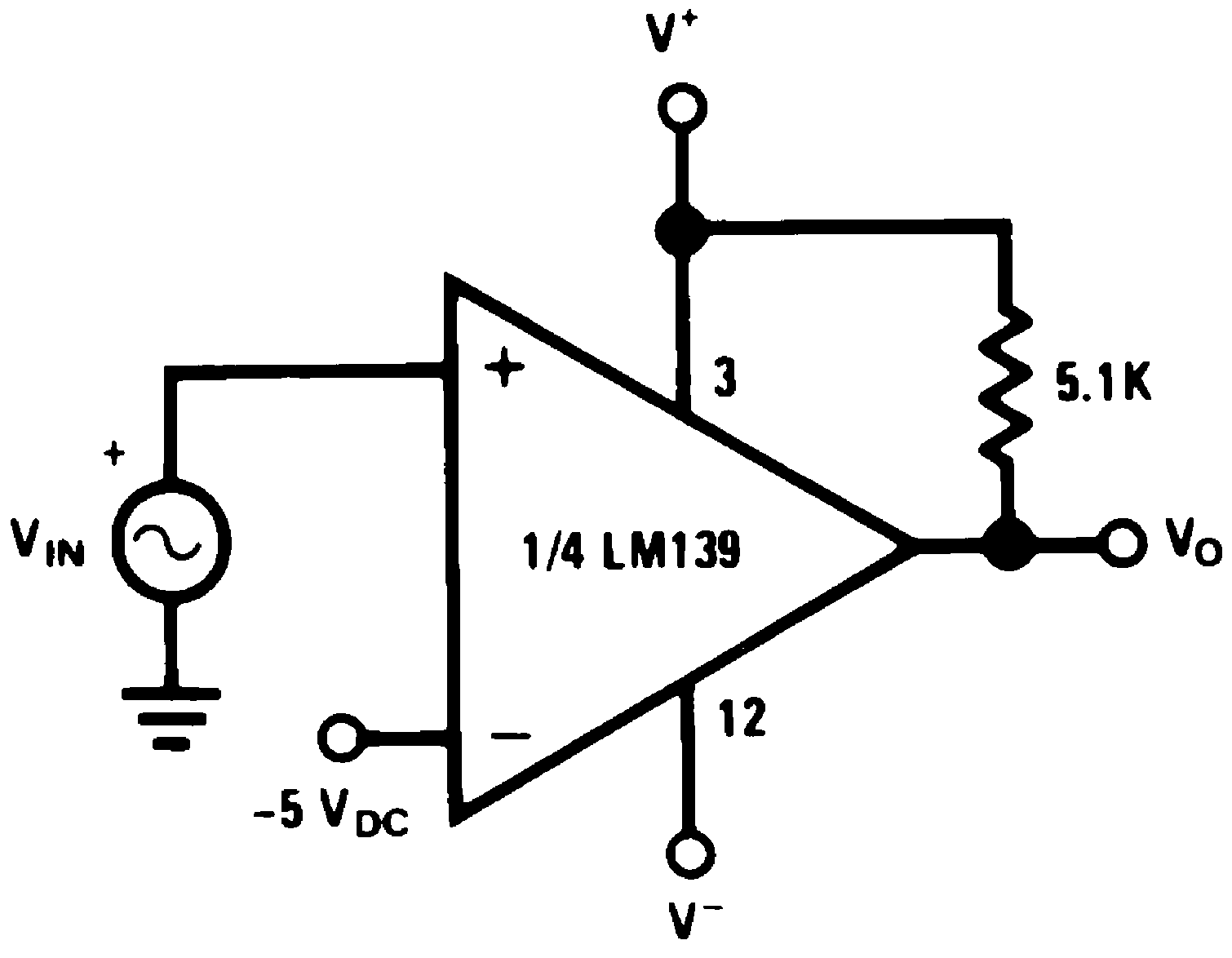
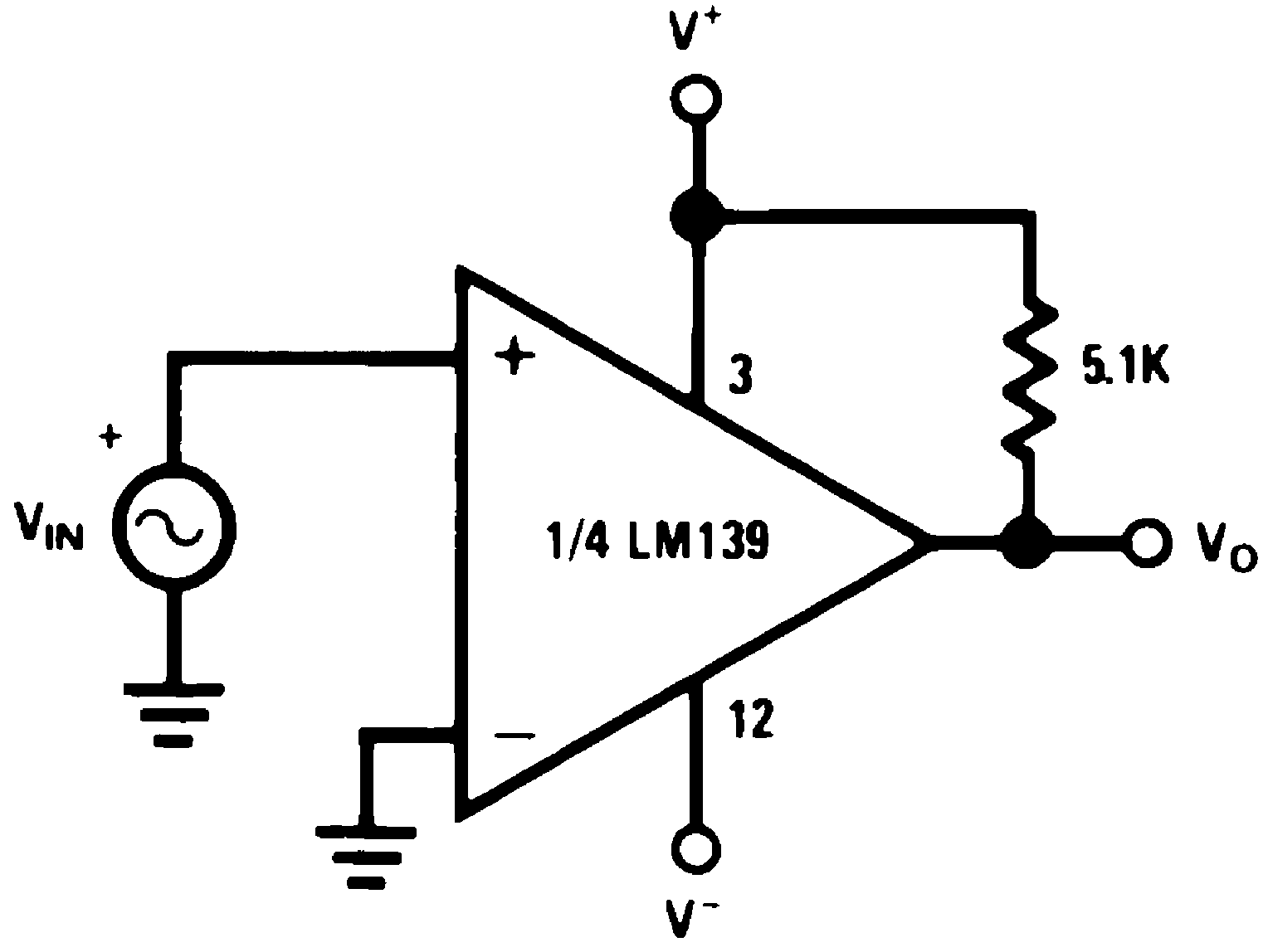
8.2.1 Basic Comparator
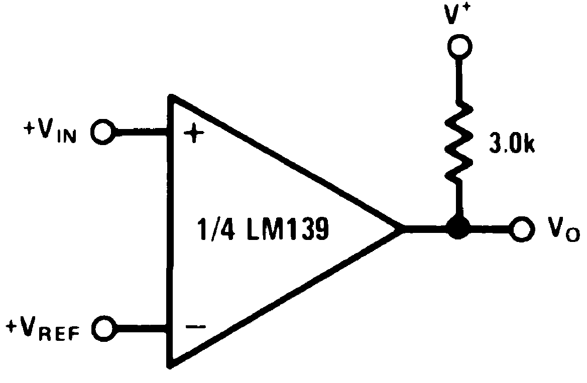 Figure 11. Basic Comparator Schematic
8.2.1.1 Design Requirements
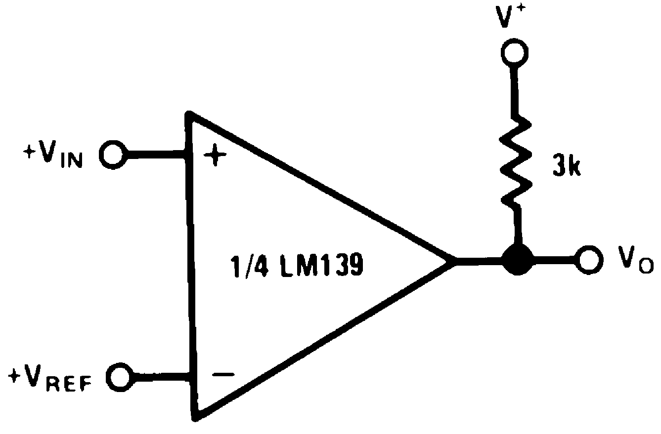
The basic usage of a comparator is to indicate when a specific analog signal has exceeded some predefined threshold. In this application, the negative input is tied to a reference voltage, and the positive input is connected to the input signal. The output is pulled up with a resistor to the logic supply voltage, V+.
For an example application, the supply voltage is 5 V. The input signal varies between 1 V and 3 V, and we want to know when the input exceeds 2.5 V. For this example, we would set the VREF to 2.5 V.
8.2.1.2 Application Curve
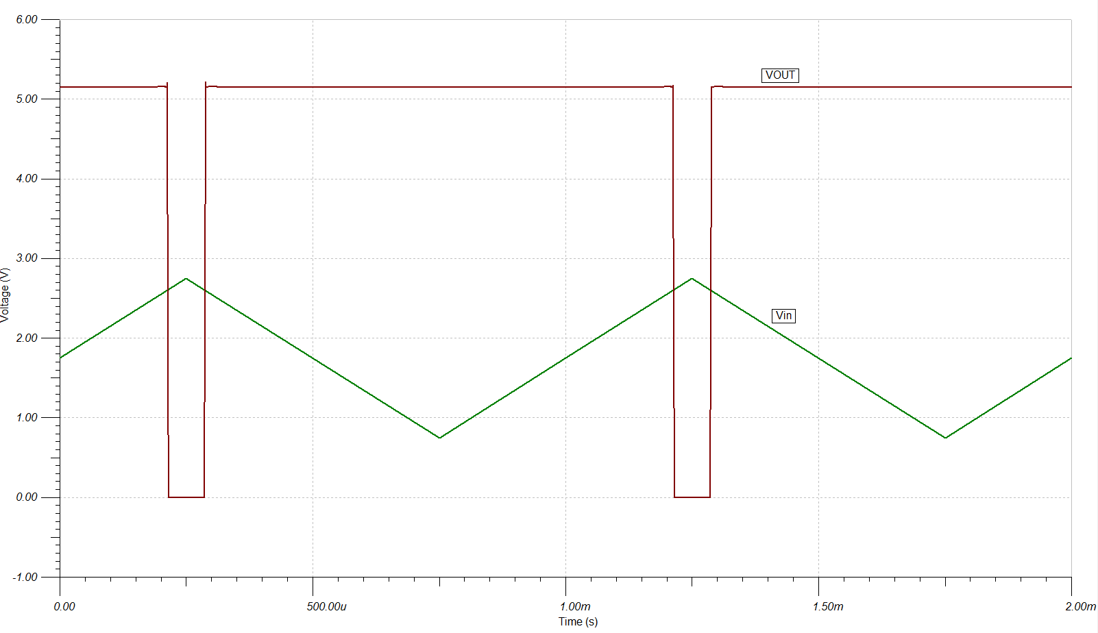 Figure 12. Basic Comparator Response
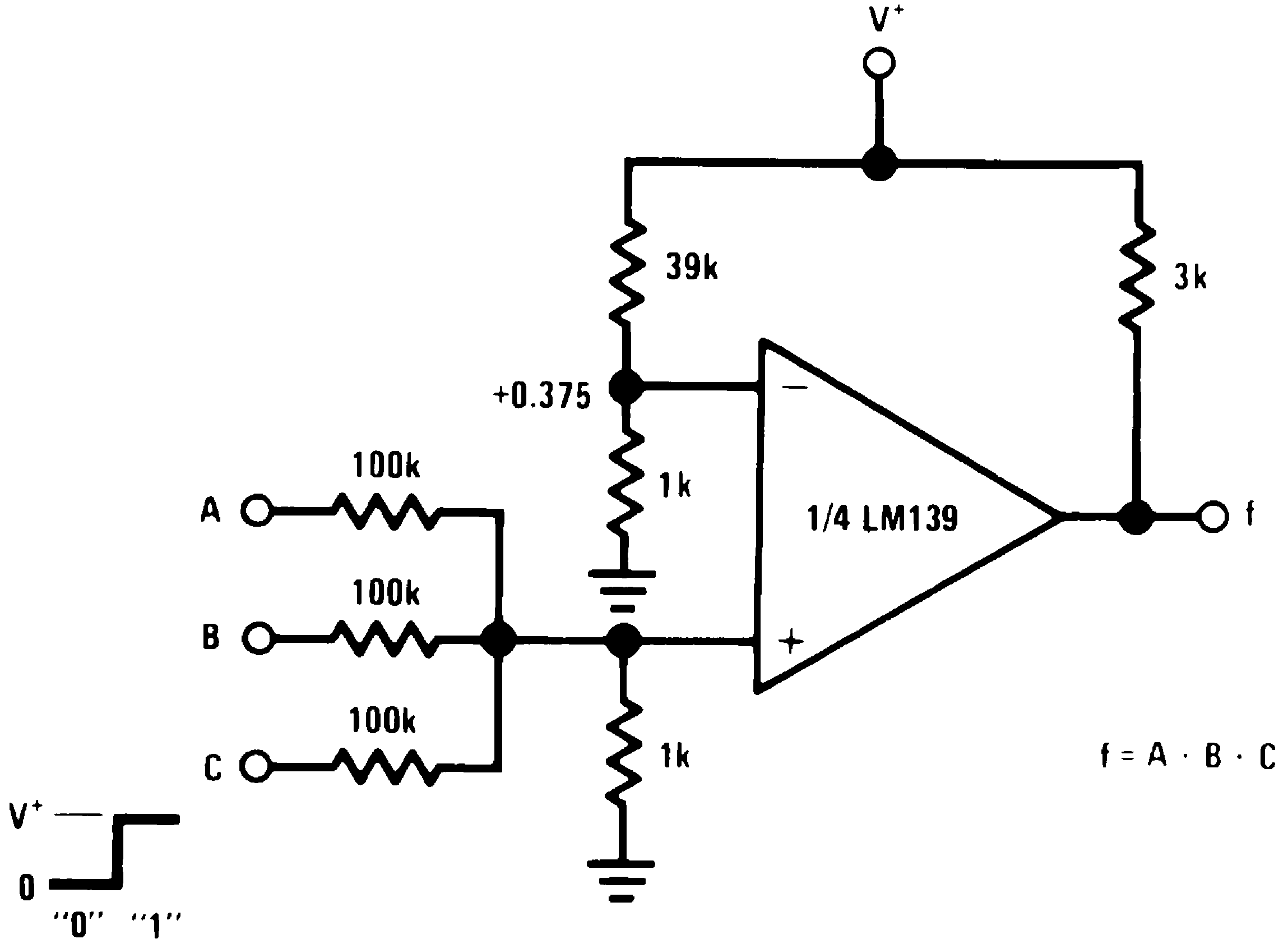
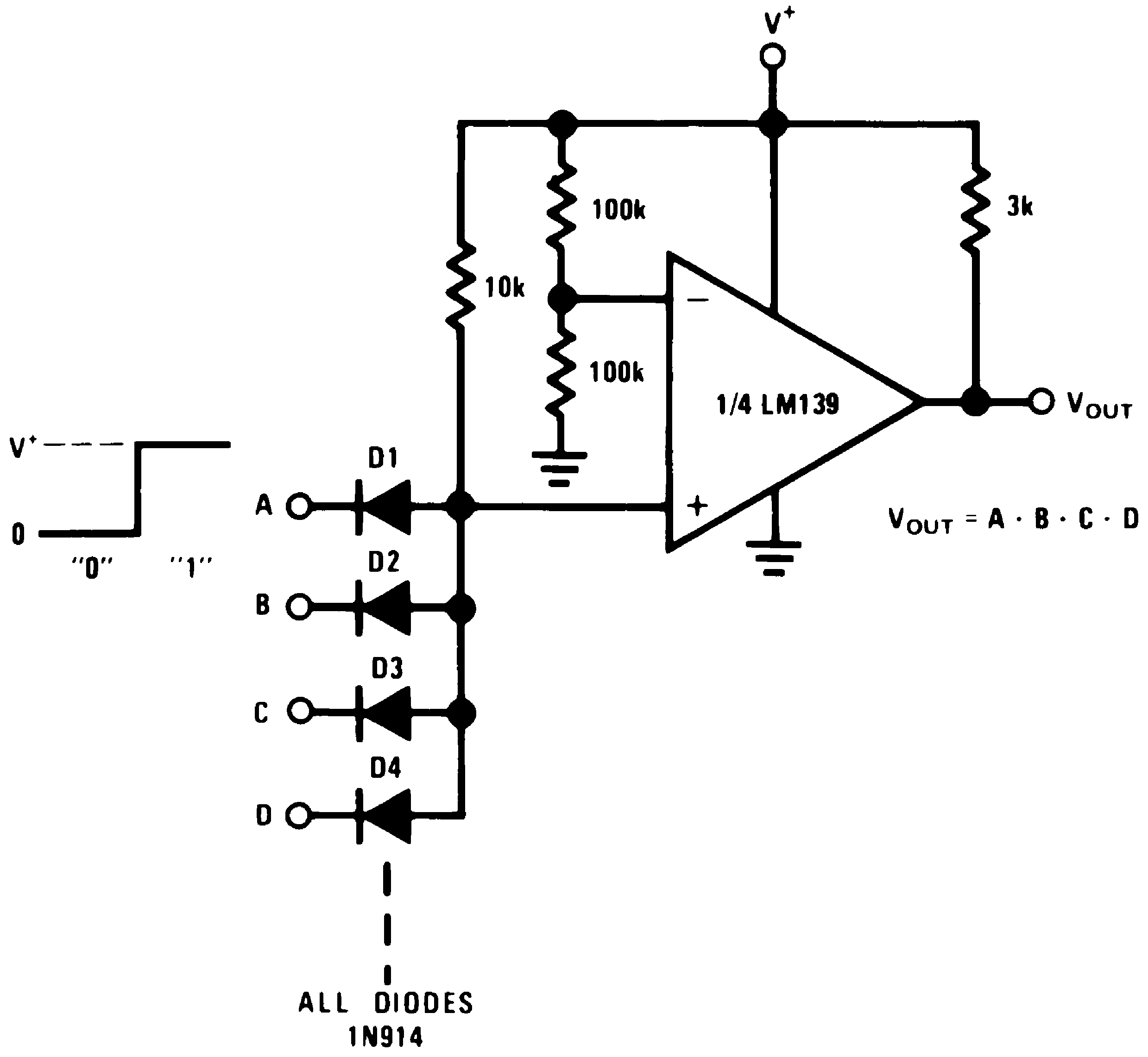
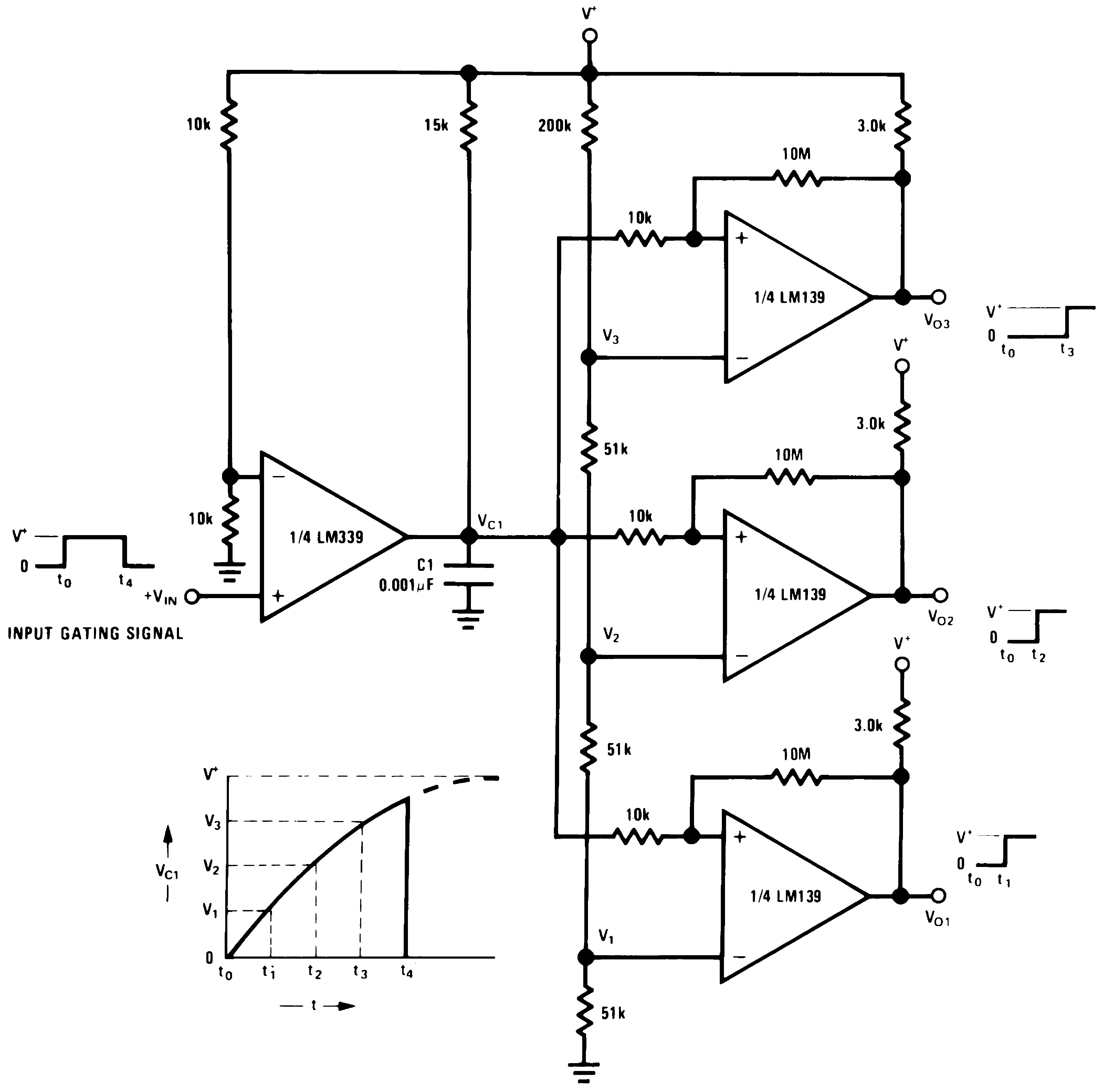
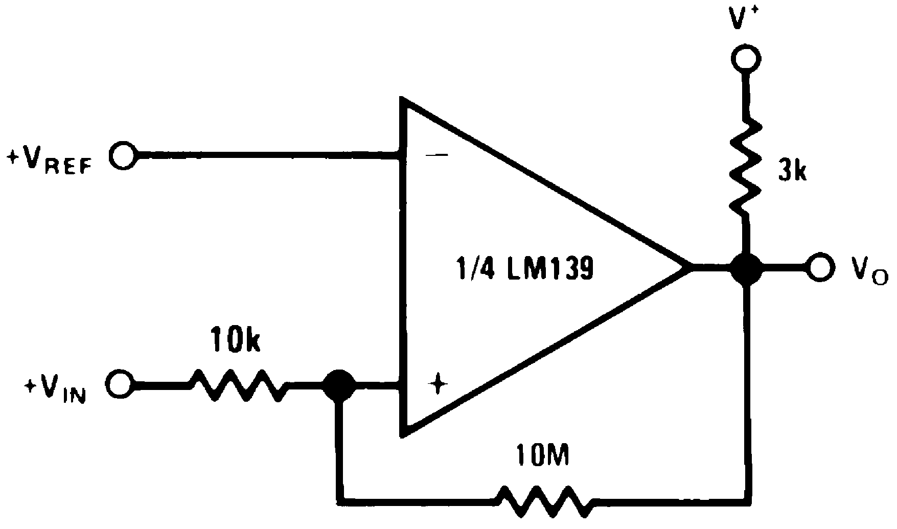
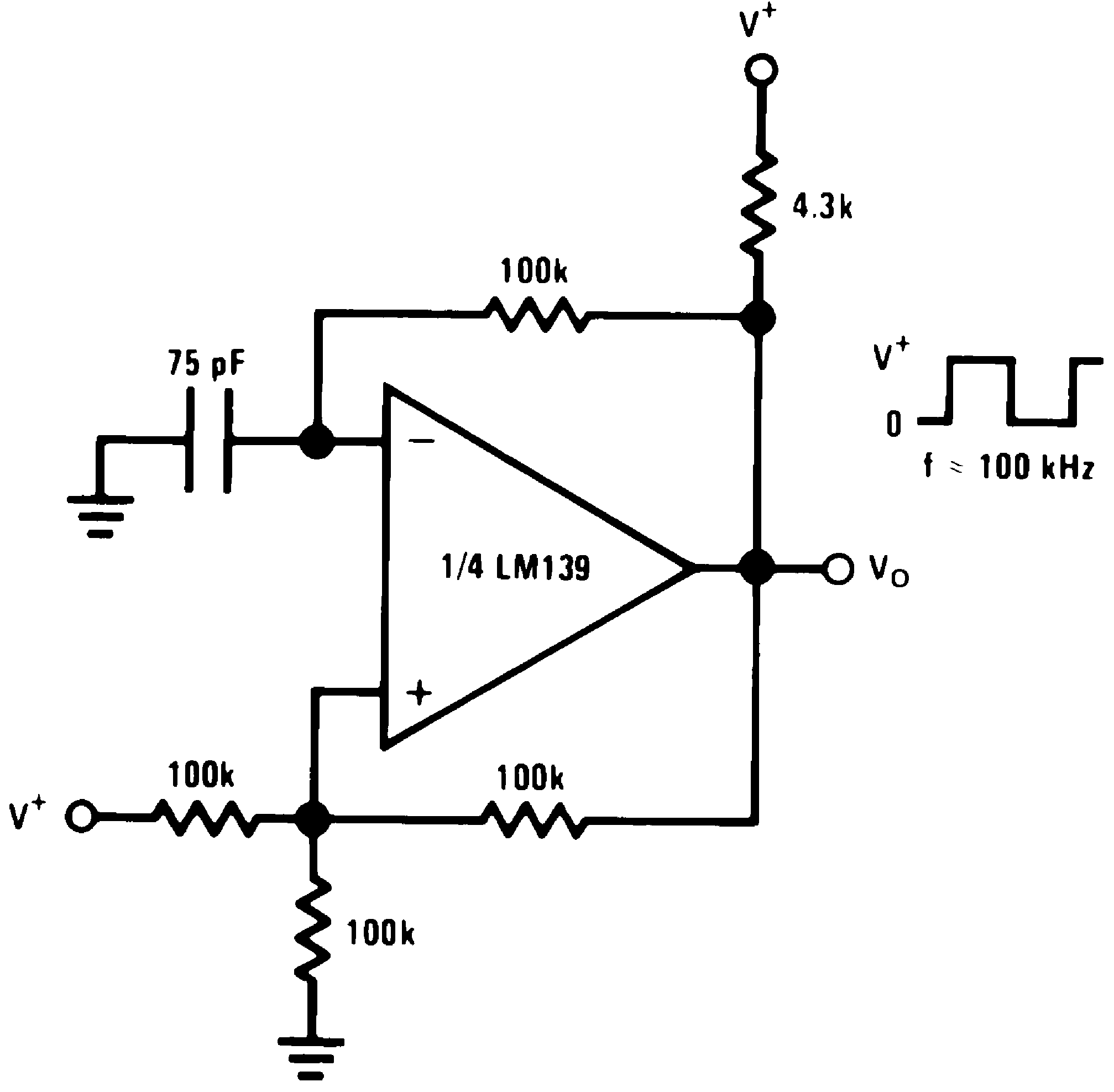
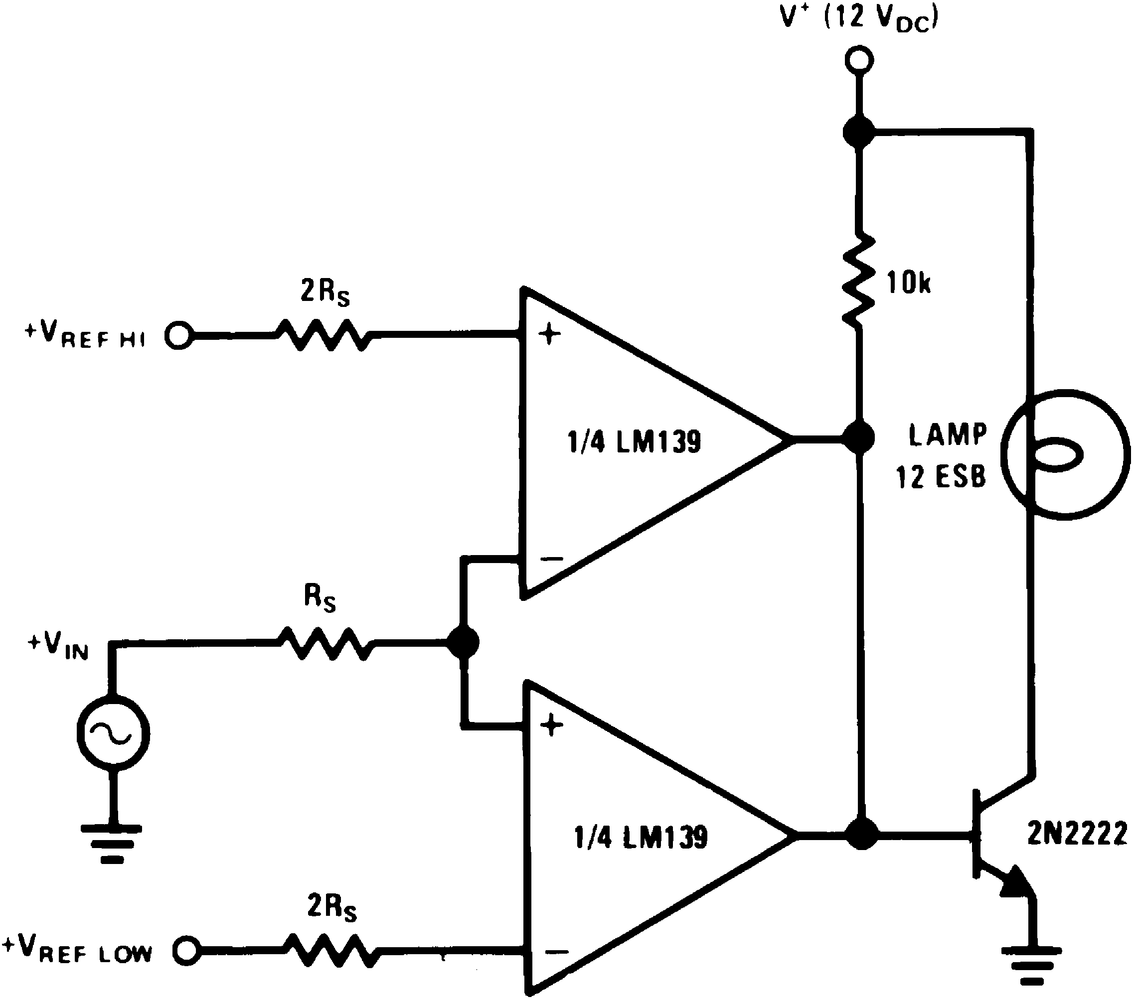
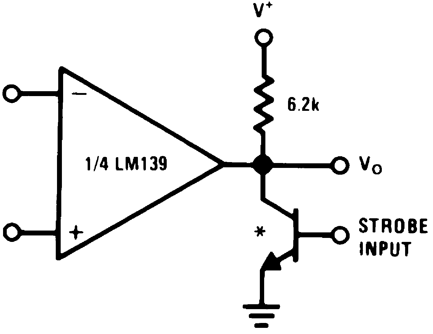
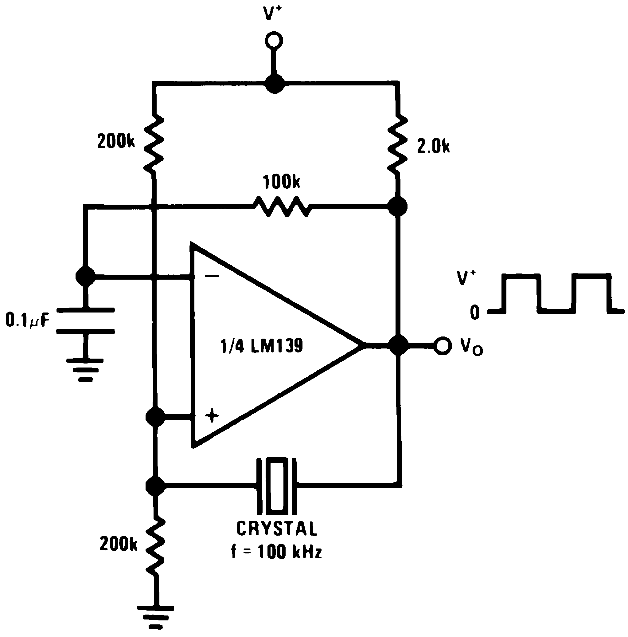
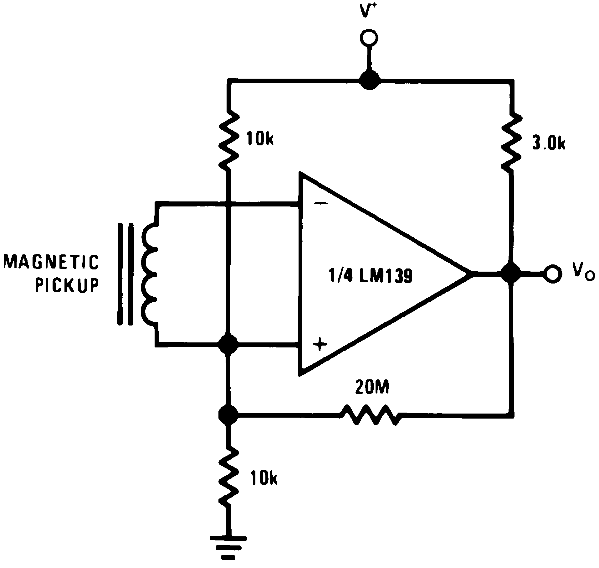
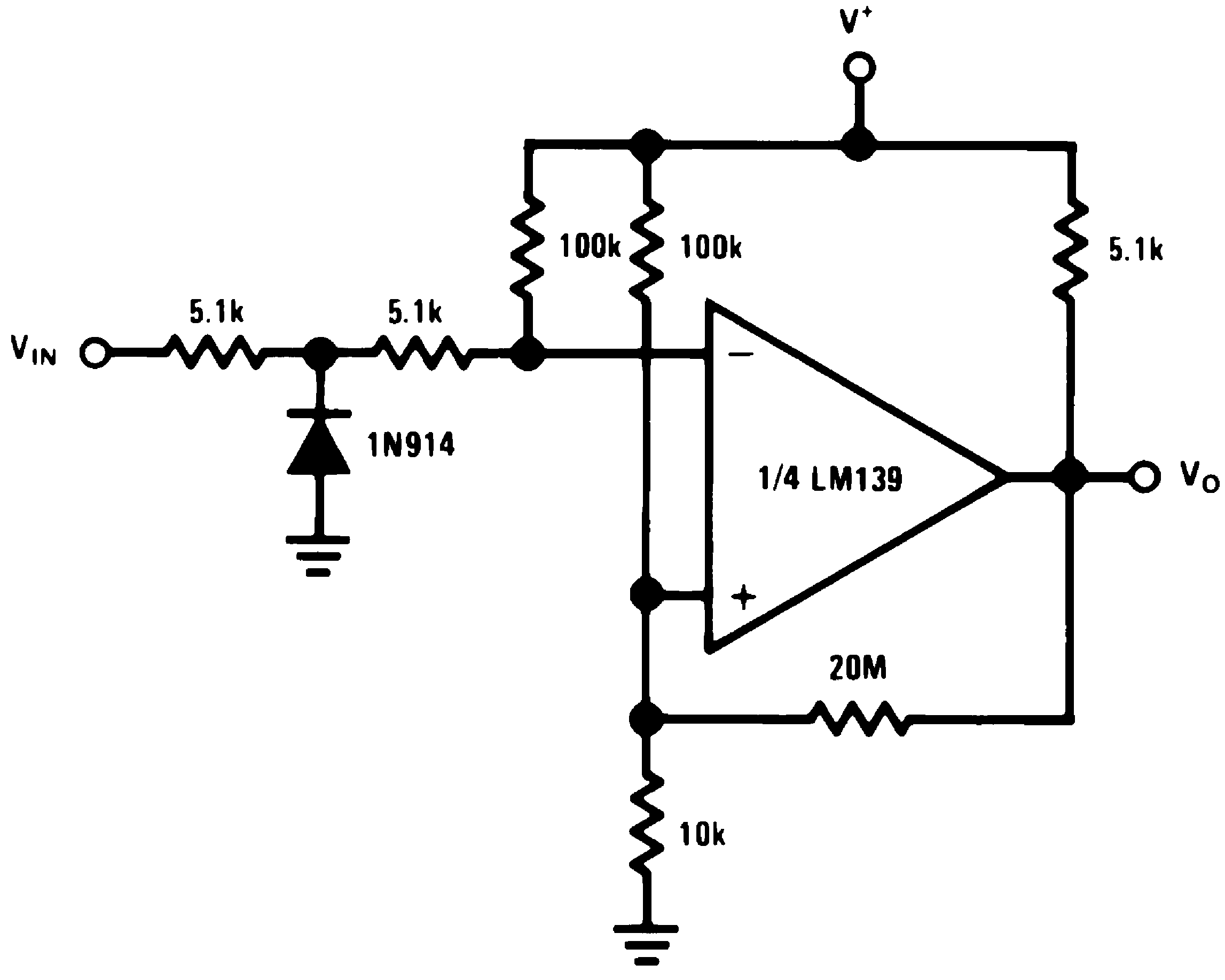
8.2.2 System Examples
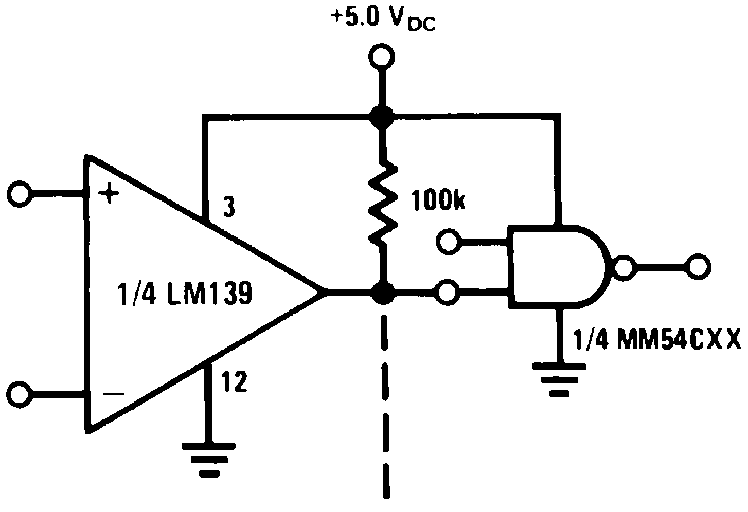
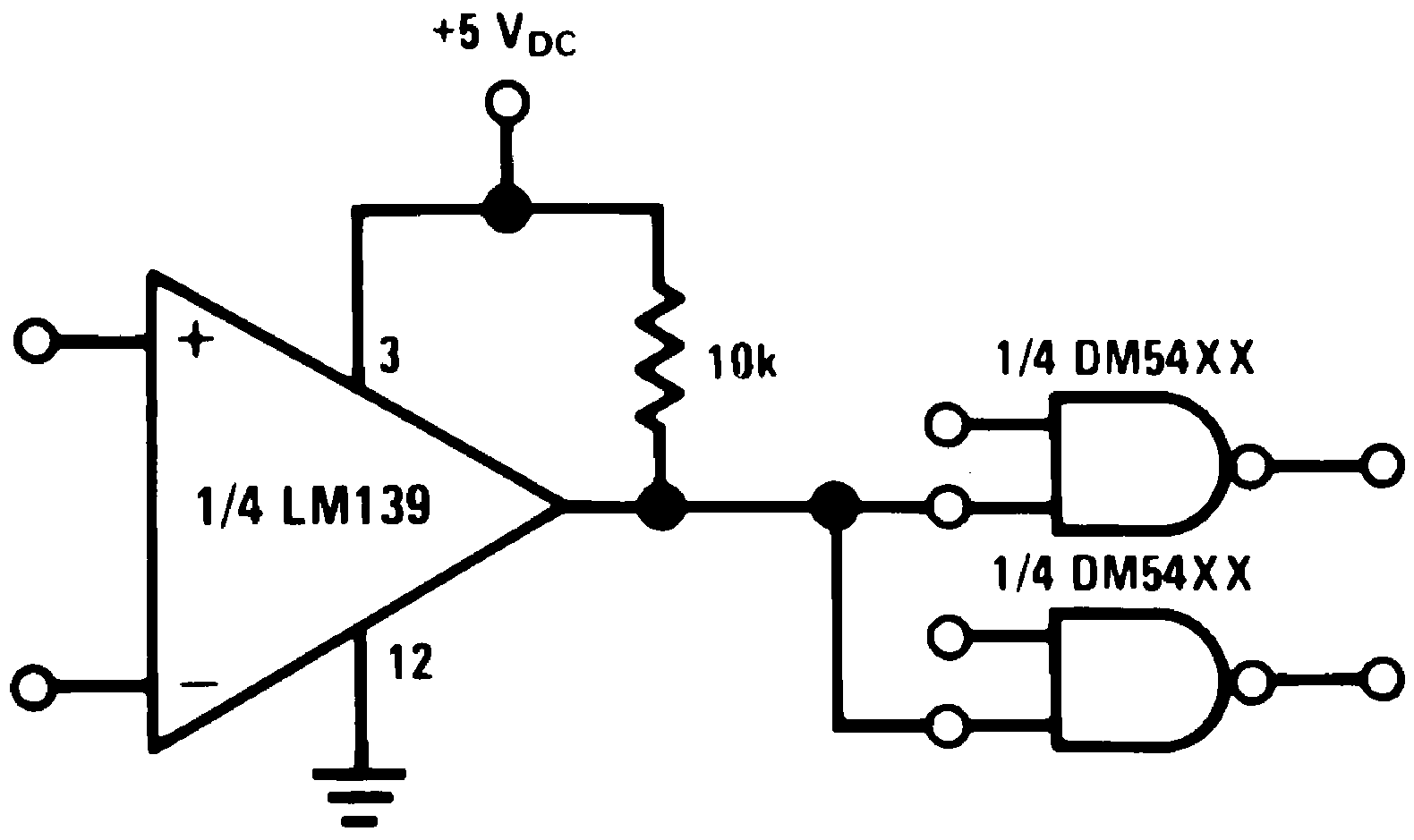
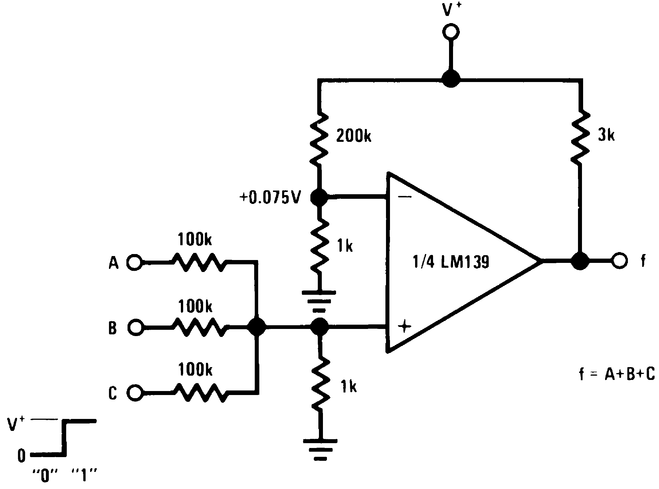
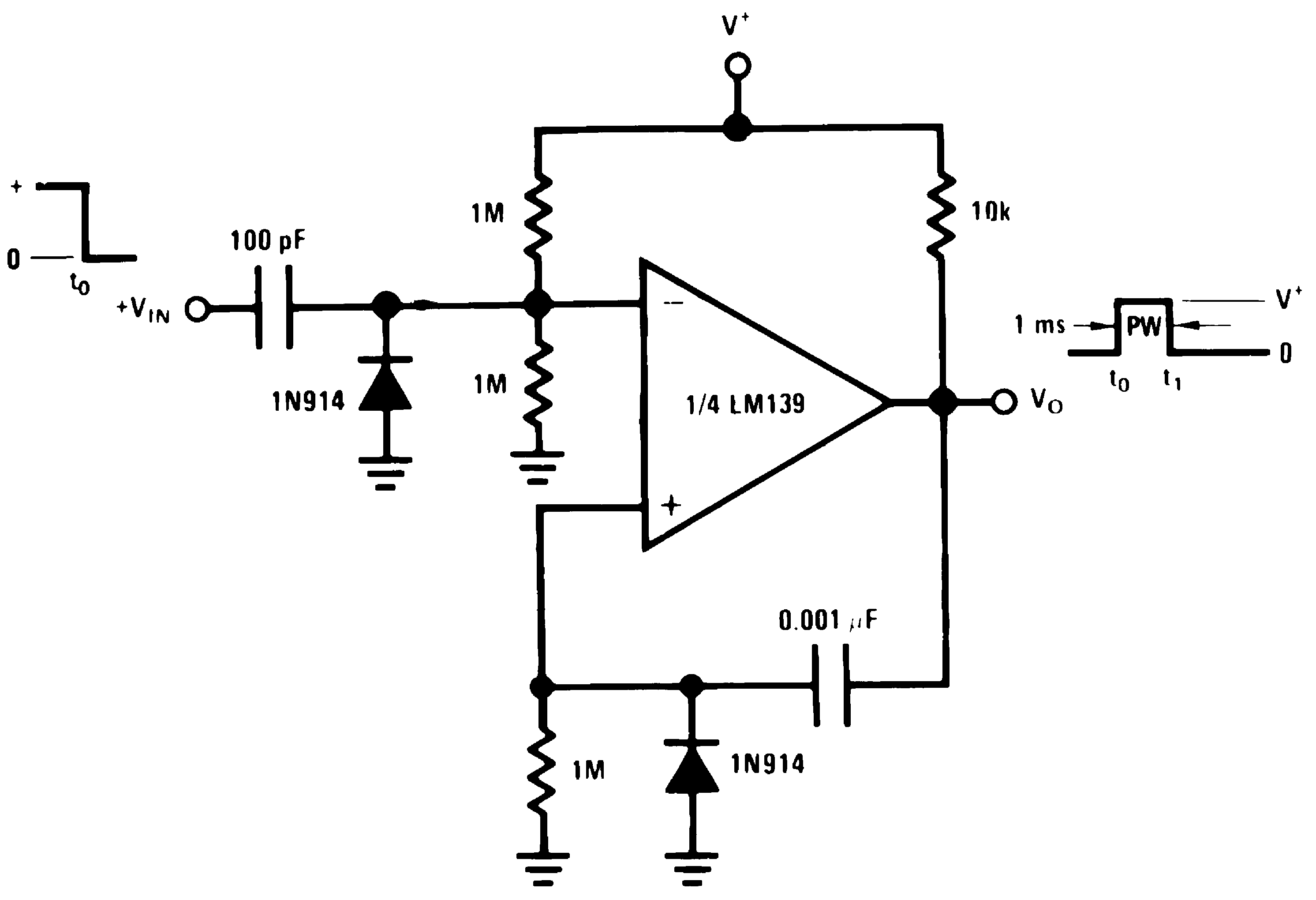
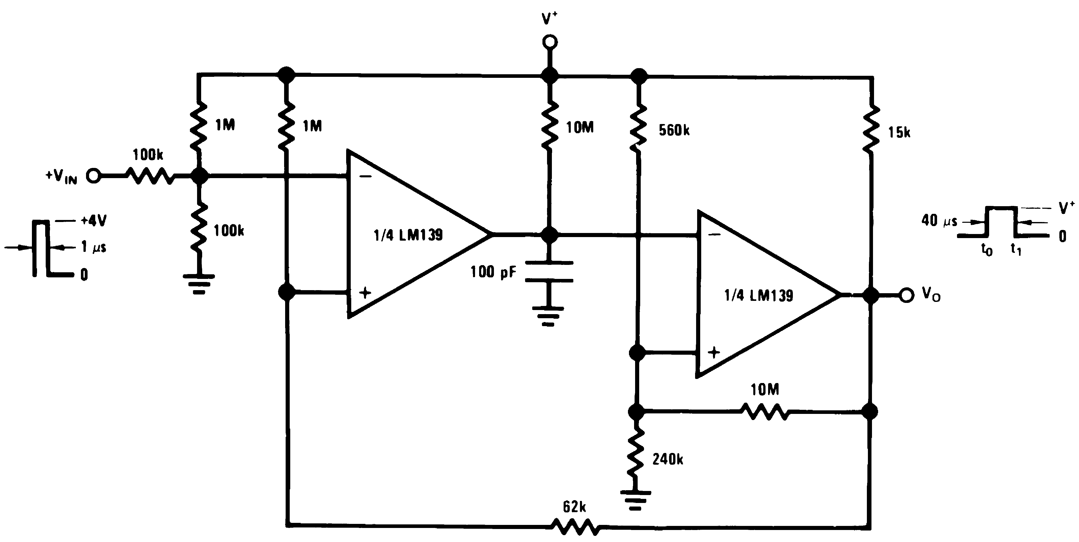
(V+ = 5.0 VDC)
(V+ = 5.0 VDC)
(V+ = 5.0 VDC)
(V+ = 5.0 VDC)
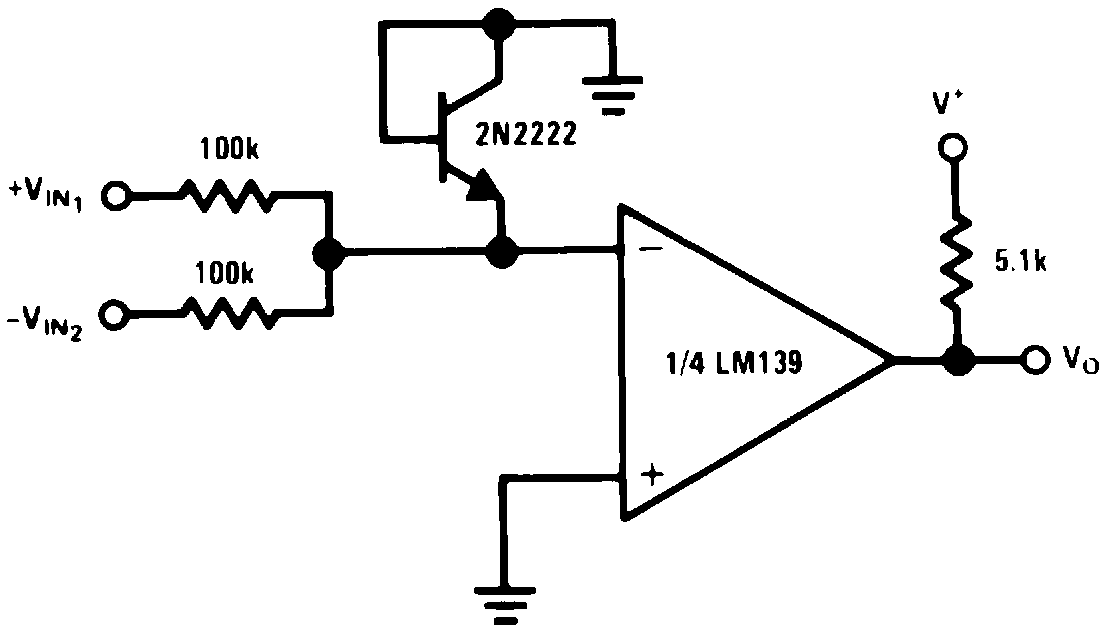
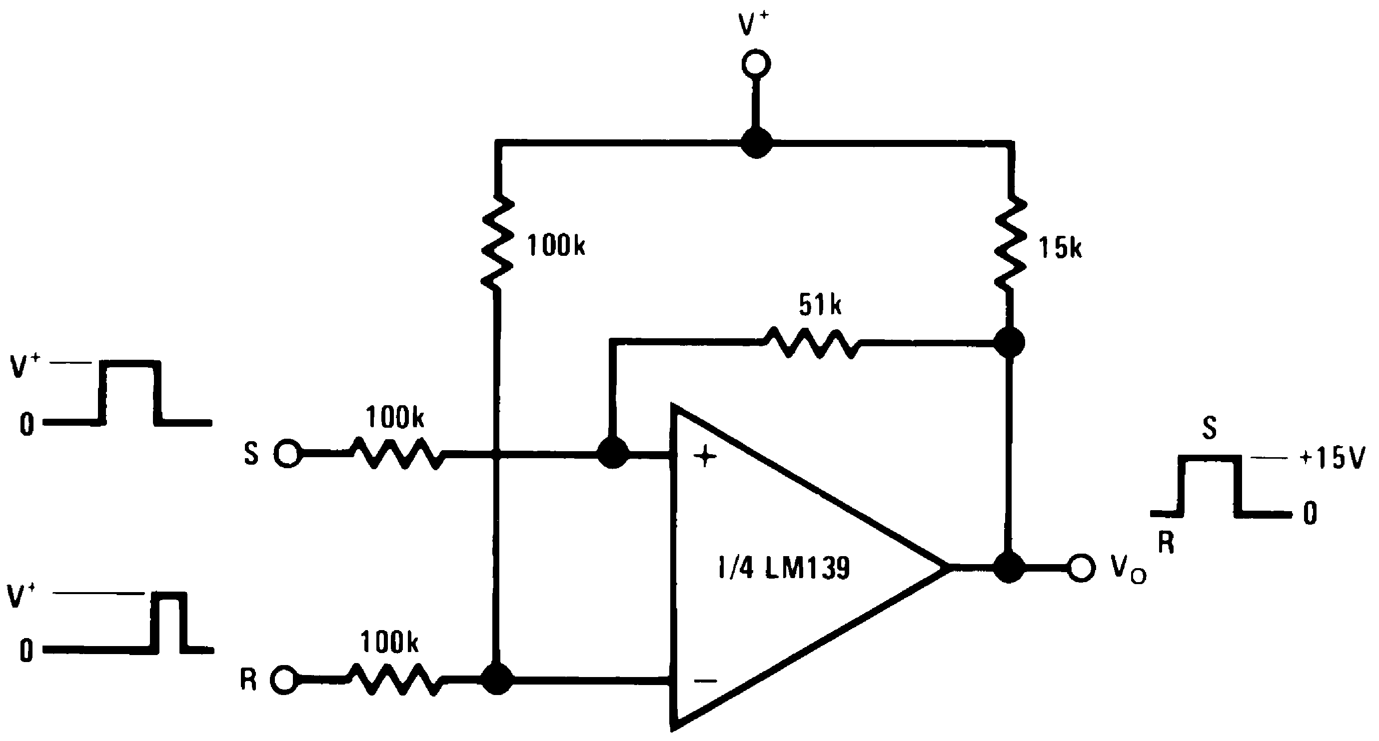
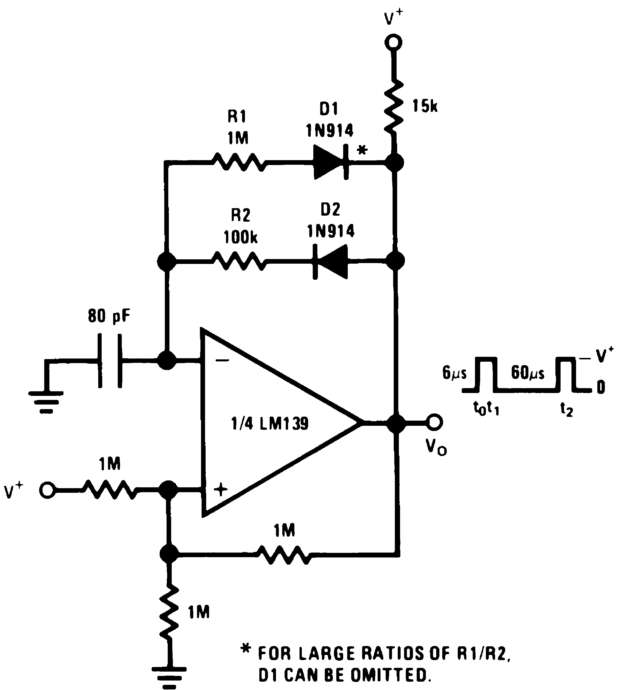
(V+= 15 VDC)
(V+= 15 VDC)
(V+= 15 VDC)
(V+= 15 VDC)
(V+= 15 VDC)
(V+= 15 VDC)
(V+= 15 VDC)
(V+= 15 VDC)
(V+= 15 VDC)
(V+= 15 VDC)
(V+= 15 VDC)
(V+= 15 VDC)
(V+= 15 VDC)
| * Or open-collector logic gate without pullup resistor | ||
(V+= 15 VDC)
(V+= 15 VDC)
(V+= 15 VDC)
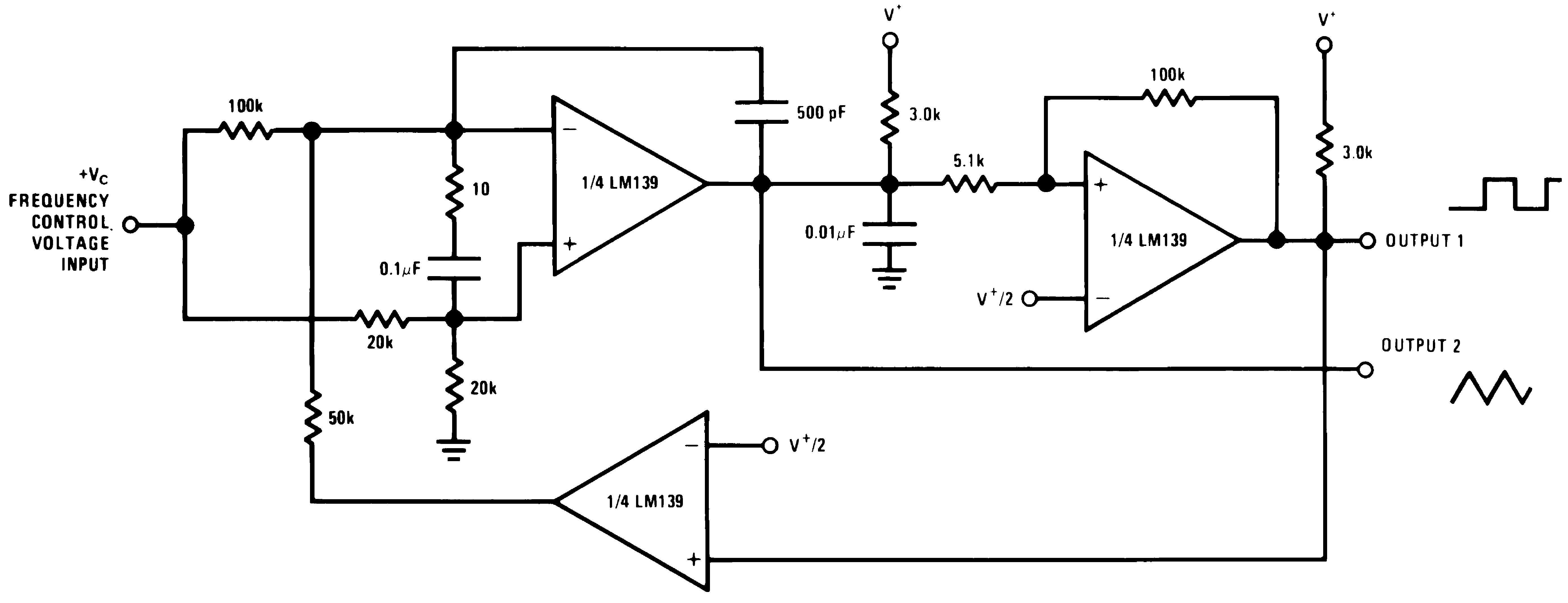
| 250 mVDC ≤ VC ≤ +50 VDC | ||
| 700 Hz ≤ fO ≤ 100 kHz |
V+ = +30 VDC
(V+= 15 VDC)
8.2.2.1 Split-Supply Applications
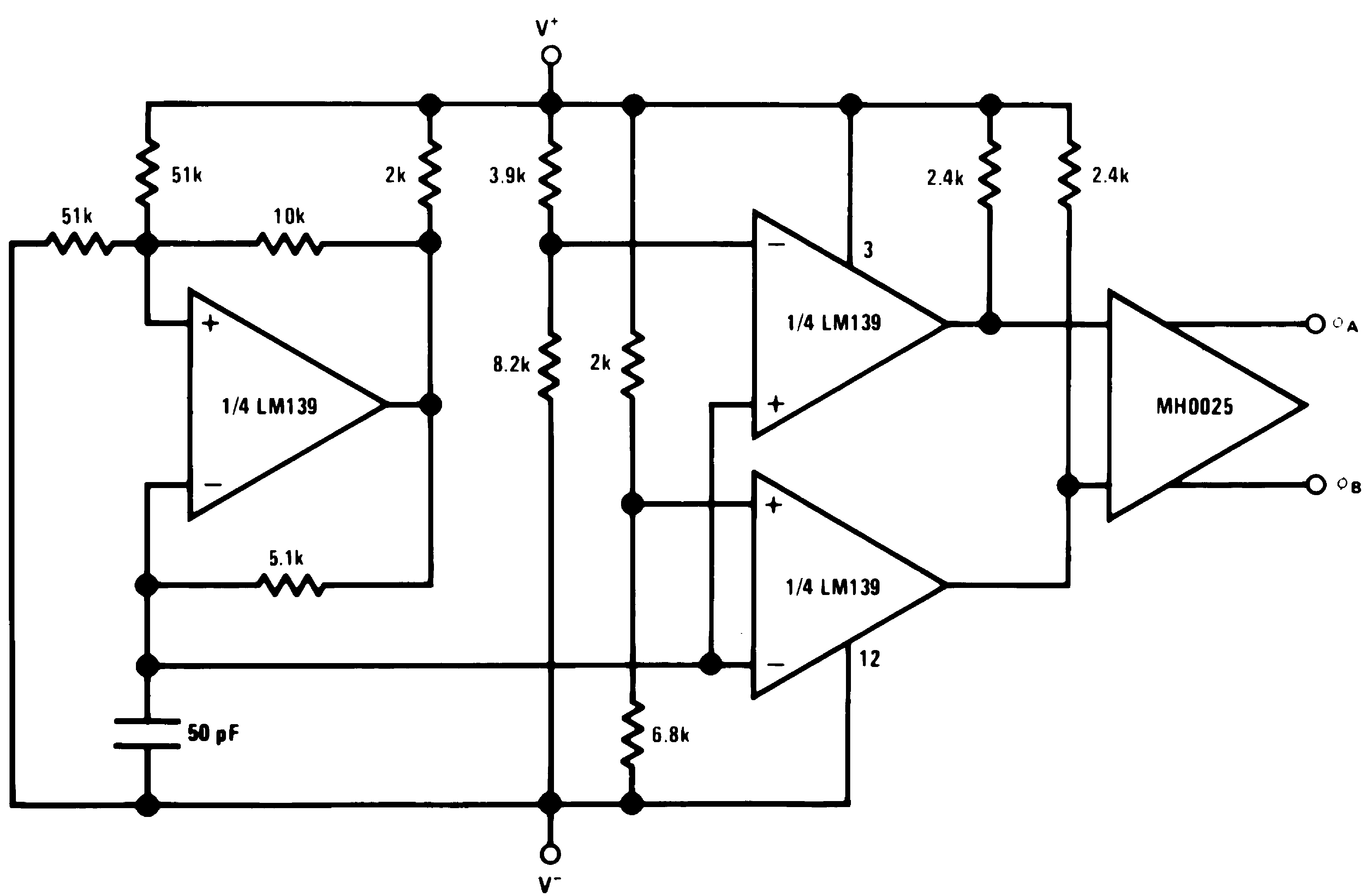
(V+ = +15 VDC and V− = −15 VDC)
(V+ = +15 VDC and V− = −15 VDC)
(V+ = +15 VDC and V− = −15 VDC)