SNOSBJ3E November 1999 – December 2014 LM139-N , LM239-N , LM2901-N , LM339-N
PRODUCTION DATA.
- 1 Features
- 2 Applications
- 3 Description
- 4 Revision History
- 5 Pin Configuration and Functions
- 6 Specifications
- 7 Detailed Description
- 8 Application and Implementation
- 9 Power Supply Recommendations
- 10Layout
- 11Device and Documentation Support
- 12Mechanical, Packaging, and Orderable Information
Package Options
Mechanical Data (Package|Pins)
Thermal pad, mechanical data (Package|Pins)
Orderable Information
6 Specifications
6.1 Absolute Maximum Ratings(1)
| MIN | MAX | UNIT | |||
|---|---|---|---|---|---|
| Supply Voltage, V+ | LM139N, LM239N, LM339N, LM2901N | 36 | VDC | ||
| LM3302N | 28 | ||||
| Differential Input Voltage | LM139N, LM239N, LM339N, LM2901N (2) | 36 | |||
| LM3302N(2) | 28 | ||||
| Input Voltage | LM139N, LM239N, LM339N, LM2901N | −0.3 | 36 | ||
| LM3302 | –0.3 | 28 | |||
| Input Current (VIN<−0.3 VDC)(3) | 50 | mA | |||
| Power Dissipation(4) | PDIP | 1050 | mW | ||
| Cavity DIP | 1190 | ||||
| SOIC Package | 760 | ||||
| Output Short-Circuit to GND(5) | Continuous | ||||
| Lead Temperature (Soldering, 10 seconds) | 260 | °C | |||
| Soldering Information | PDIP Package (10 seconds) | 260 | |||
| SOIC Package | Vapor Phase (60 seconds) | 215 | |||
| Infrared (15 seconds) | 220 | ||||
| Storage temperature, Tstg | −65 | 150 | |||
(1) Refer to RETS139AX for LM139A military specifications and to RETS139X for LM139 military specifications.
(2) Positive excursions of input voltage may exceed the power supply level. As long as the other voltage remains within the common-mode range, the comparator will provide a proper output state. The low input voltage state must not be less than −0.3 VDC (or 0.3 VDC below the magnitude of the negative power supply, if used) (at 25°C).
(3) This input current will only exist when the voltage at any of the input leads is driven negative. It is due to the collector-base junction of the input PNP transistors becoming forward biased and thereby acting as input diode clamps. In addition to this diode action, there is also lateral NPN parasitic transistor action on the IC chip. This transistor action can cause the output voltages of the comparators to go to the V+ voltage level (or to ground for a large overdrive) for the time duration that an input is driven negative. This is not destructive and normal output states will re-establish when the input voltage, which was negative, again returns to a value greater than −0.3 VDC (at 25°C).
(4) For operating at high temperatures, the LM339/LM339A, LM2901, LM3302 must be derated based on a 125°C maximum junction temperature and a thermal resistance of 95°C/W which applies for the device soldered in a printed circuit board, operating in a still air ambient. The LM239-N and LM139-N must be derated based on a 150°C maximum junction temperature. The low bias dissipation and the “ON-OFF” characteristic of the outputs keeps the chip dissipation very small (PD≤100 mW), provided the output transistors are allowed to saturate.
(5) Short circuits from the output to V+ can cause excessive heating and eventual destruction. When considering short circuits to ground, the maximum output current is approximately 20 mA independent of the magnitude of V+.
6.2 ESD Ratings
| VALUE | UNIT | |||
|---|---|---|---|---|
| V(ESD) | Electrostatic discharge | Human-body model (HBM), per ANSI/ESDA/JEDEC JS-001(1) | ±600 | V |
(1) JEDEC document JEP155 states that 500-V HBM allows safe manufacturing with a standard ESD control process.
6.3 Recommended Operating Conditions
over operating free-air temperature range (unless otherwise noted)| MIN | MAX | UNIT | |||
|---|---|---|---|---|---|
| Supply Voltage | Single Supply | LM139N, LM239N, LM339N, LM2901N | 2 | 36 | V |
| LM3302N | 2 | 28 | |||
| Dual Supply | LM139N, LM239N, LM339N, LM2901N | ±1 | ±18 | ||
| LM3302N | ±1 | ±14 | |||
| Operating Temperature | LM139/LM139A | −55 | 125 | °C | |
| LM2901/LM3302 | −40 | 85 | |||
| LM239/LM239A | −25 | 85 | |||
| LM339/LM339A | 0 | 70 | |||
6.4 Thermal Information
| THERMAL METRIC(1) | LM139-N, LM239-N, LM339-N | LM2901-N, LM339-N | LM2901-N, LM339-N | UNIT | |
|---|---|---|---|---|---|
| J | D | NFF | |||
| 14 PINS | |||||
| RθJA | Junction-to-ambient thermal resistance | 95 | 95 | 95 | °C/W |
(1) For more information about traditional and new thermal metrics, see the IC Package Thermal Metrics application report, SPRA953.
6.5 Electrical Characteristics: LM139A, LM239A, LM339A, LM139
(V+=5 VDC, TA = 25°C(1) unless otherwise stated)| PARAMETER | TEST CONDITIONS | LM139A | LM239A, LM339A | LM139 | UNIT | ||||||
|---|---|---|---|---|---|---|---|---|---|---|---|
| MIN | TYP | MAX | MIN | TYP | MAX | MIN | TYP | MAX | |||
| Input Offset Voltage | See(2) | 1.0 | 2.0 | 1.0 | 2.0 | 2.0 | 5.0 | mVDC | |||
| Input Bias Current | IIN(+) or IIN(−) with Output in Linear Range(3), VCM=0 V | 25 | 100 | 25 | 250 | 25 | 100 | nADC | |||
| Input Offset Current | IIN(+) − IIN(−), VCM= 0 V | 3.0 | 25 | 5.0 | 50 | 3.0 | 25 | nADC | |||
| Input Common-Mode Voltage Range | V+=30 VDC (LM3302, | 0 | V+−1.5 | 0 | V+−1.5 | 0 | V+−1.5 | VDC | |||
| V+ = 28 VDC)(4) | |||||||||||
| Supply Current | (LM3302, V+ = 28 VDC), RL = ∞ on all Comparators | 0.8 | 2.0 | 0.8 | 2.0 | 0.8 | 2.0 | mADC | |||
| (LM3302, V+ = 28 VDC), RL = ∞, V+ = 36 V | 1.0 | 2.5 | 1.0 | 2.5 | mADC | ||||||
| Voltage Gain | RL≥15 kΩ, V+ = 15 VDC | 50 | 200 | 50 | 200 | 50 | 200 | V/mV | |||
| VO = 1 VDC to 11 VDC | |||||||||||
| Large Signal Response Time | VIN = TTL Logic Swing, VREF = | 300 | 300 | 300 | ns | ||||||
| 1.4 VDC, VRL = 5 VDC, | |||||||||||
| RL = 5.1 kΩ | |||||||||||
| Response Time | VRL = 5 VDC, RL = 5.1 kΩ(5) | 1.3 | 1.3 | 1.3 | μs | ||||||
| Output Sink Current | VIN(−) = 1 VDC, VIN(+) = 0, | 6.0 | 16 | 6.0 | 16 | 6.0 | 16 | mADC | |||
| VO ≤ 1.5 VDC | |||||||||||
| Saturation Voltage | VIN(−) = 1 VDC, VIN(+) = 0, | 250 | 400 | 250 | 400 | 250 | 400 | mVDC | |||
| ISINK ≤ 4 mA | |||||||||||
| Output Leakage Current | VIN(+) = 1 VDC, VIN(−) = 0, | 0.1 | 0.1 | 0.1 | nADC | ||||||
| VO = 5 VDC | |||||||||||
| Input Offset Voltage | See(2) | 4.0 | 4.0 | 9.0 | mVDC | ||||||
| Input Offset Current | IIN(+)−IIN(−), VCM = 0 V | 100 | 150 | 100 | nADC | ||||||
| Input Bias Current | IIN(+) or IIN(−) with Output in | 300 | 400 | 300 | nADC | ||||||
| Linear Range, VCM = 0 V(3) | |||||||||||
| Input Common-Mode | V+=30 VDC (LM3302), | 0 | V+−2.0 | 0 | V+−2.0 | 0 | V+−2.0 | VDC | |||
| Voltage Range | V+ = 28 VDC)(4) | ||||||||||
| Saturation Voltage | VIN(−)=1 VDC, VIN(+) = 0, ISINK ≤ 4 mA |
700 | 700 | 700 | mVDC | ||||||
| Output Leakage Current | VIN(+) = 1 VDC, VIN(−) = 0, VO = 30 VDC, (LM3302, VO = 28 VDC) |
1.0 | 1.0 | 1.0 | μADC | ||||||
| Differential Input Voltage | Keep all VIN's ≥ 0 VDC (or V−, if used)(6) | 36 | 36 | 36 | VDC | ||||||
(1) These specifications are limited to −55°C ≤ TA ≤ 125°C, for the LM139/LM139A. With the LM239/LM239A, all temperature specifications are limited to −25°C ≤ TA ≤ 85°C, the LM339/LM339A temperature specifications are limited to 0°C ≤ TA ≤ 70°C, and the LM2901, LM3302 temperature range is −40°C ≤ TA ≤ 85°C.
(2) At output switch point, VO≃1.4 VDC, RS = 0 Ω with V+ from 5 VDC to 30 VDC; and over the full input common-mode range (0 VDC to V+ −1.5 VDC), at 25°C. For LM3302, V+ from 5 VDC to 28 VDC.
(3) The direction of the input current is out of the IC due to the PNP input stage. This current is essentially constant, independent of the state of the output so no loading change exists on the reference or input lines.
(4) The input common-mode voltage or either input signal voltage should not be allowed to go negative by more than 0.3 V. The upper end of the common-mode voltage range is V+ −1.5V at 25°C, but either or both inputs can go to 30 VDC without damage (25V for LM3302), independent of the magnitude of V+.
(5) The response time specified is a 100-mV input step with 5-mV overdrive. For larger overdrive signals 300 ns can be obtained, see typical performance characteristics section.
(6) Positive excursions of input voltage may exceed the power supply level. As long as the other voltage remains within the common-mode range, the comparator will provide a proper output state. The low input voltage state must not be less than −0.3 VDC (or 0.3 VDCbelow the magnitude of the negative power supply, if used) (at 25°C).
6.6 Electrical Characteristics: LM239, LM339, LM2901, LM3302
(V+ = 5 VDC, TA = 25°C(1) unless otherwise stated)| PARAMETER | TEST CONDITIONS | LM239, LM339 | LM2901 | LM3302 | UNIT | ||||||
|---|---|---|---|---|---|---|---|---|---|---|---|
| MIN | TYP | MAX | MIN | TYP | MAX | MIN | TYP | MAX | |||
| Input Offset Voltage | See(2) | 2.0 | 5.0 | 2.0 | 7.0 | 3 | 20 | mVDC | |||
| Input Bias Current | IIN(+) or IIN(−) with Output in Linear Range(3), VCM=0 V | 25 | 250 | 25 | 250 | 25 | 500 | nADC | |||
| Input Offset Current | IIN(+)−IIN(−), VCM = 0 V | 5.0 | 50 | 5 | 50 | 3 | 100 | nADC | |||
| Input Common-Mode Voltage Range | V+ = 30 VDC (LM3302, V+ = 28 VDC)(4) |
0 | V+−1.5 | 0 | V+−1.5 | 0 | V+−1.5 | VDC | |||
| Supply Current | (LM3302, V+ = 28 VDC) RL = ∞ on all Comparators | 0.8 | 2.0 | 0.8 | 2.0 | 0.8 | 2.0 | mADC | |||
| (LM3302, V+ = 28 VDC) RL = ∞, V+ = 36 V | 1.0 | 2.5 | 1.0 | 2.5 | 1.0 | 2.5 | mADC | ||||
| Voltage Gain | RL ≥ 15 kΩ, V+ = 15 VDC | 50 | 200 | 25 | 100 | 2 | 30 | V/mV | |||
| VO = 1 VDC to 11 VDC | |||||||||||
| Large Signal Response Time | VIN = TTL Logic Swing, VREF = | 300 | 300 | 300 | ns | ||||||
| 1.4 VDC, VRL = 5 VDC, | |||||||||||
| RL = 5.1 kΩ, | |||||||||||
| Response Time | VRL = 5 VDC, RL = 5.1 kΩ(5) | 1.3 | 1.3 | 1.3 | μs | ||||||
| Output Sink Current | VIN(−)= 1 VDC, VIN(+) = 0, | 6.0 | 16 | 6.0 | 16 | 6.0 | 16 | mADC | |||
| VO ≤ 1.5 VDC | |||||||||||
| Saturation Voltage | VIN(−) = 1 VDC, VIN(+) = 0, | 250 | 400 | 250 | 400 | 250 | 500 | mVDC | |||
| ISINK ≤ 4 mA | |||||||||||
| Output Leakage Current | VIN(+) = 1 VDC,VIN(−) = 0, | 0.1 | 0.1 | 0.1 | nADC | ||||||
| VO = 5 VDC | |||||||||||
| Input Offset Voltage | See(2) | 9.0 | 9 | 15 | 40 | mVDC | |||||
| Input Offset Current | IIN(+)− IIN(−), VCM = 0 V | 150 | 50 | 200 | 300 | nADC | |||||
| Input Bias Current | IIN(+) or IIN(−) with Output in | 400 | 200 | 500 | 1000 | nADC | |||||
| Linear Range, VCM = 0V(3) | |||||||||||
| Input Common-Mode | V+ = 30 VDC (LM3302, V+ = 28 VDC) | V+−2.0 | 0 | V+−2.0 | 0 | V+−2.0 | VDC | ||||
| Voltage Range | See(4) | ||||||||||
| Saturation Voltage | VIN(−) = 1 VDC, VIN(+) = 0, ISINK ≤ 4 mA |
700 | 400 | 700 | 700 | mVDC | |||||
| Output Leakage Current | VIN(+) = 1 VDC, VIN(−) = 0, VO = 30 VDC, (LM3302, V O = 28 VDC) | 1.0 | 1.0 | 1.0 | μADC | ||||||
| Differential Input Voltage | Keep all VIN's ≥ 0 VDC (or V−, if used)(6) | 36 | 36 | 28 | VDC | ||||||
(1) These specifications are limited to −55°C ≤ TA ≤ 125°C, for the LM139/LM139A. With the LM239/LM239A, all temperature specifications are limited to −25°C ≤ TA ≤ 85°C, the LM339/LM339A temperature specifications are limited to 0°C ≤ TA ≤ 70°C, and the LM2901, LM3302 temperature range is −40°C ≤ TA ≤ 85°C.
(2) At output switch point, VO≃1.4 VDC, RS = 0 Ω with V+ from 5 VDC to 30 VDC; and over the full input common-mode range (0 VDC to V+ −1.5 VDC), at 25°C. For LM3302, V+ from 5 VDC to 28 VDC.
(3) The direction of the input current is out of the IC due to the PNP input stage. This current is essentially constant, independent of the state of the output so no loading change exists on the reference or input lines.
(4) The input common-mode voltage or either input signal voltage should not be allowed to go negative by more than 0.3 V. The upper end of the common-mode voltage range is V+ −1.5V at 25°C, but either or both inputs can go to 30 VDC without damage (25V for LM3302), independent of the magnitude of V+.
(5) The response time specified is a 100-mV input step with 5-mV overdrive. For larger overdrive signals 300 ns can be obtained, see typical performance characteristics section.
(6) Positive excursions of input voltage may exceed the power supply level. As long as the other voltage remains within the common-mode range, the comparator will provide a proper output state. The low input voltage state must not be less than −0.3 VDC (or 0.3 VDCbelow the magnitude of the negative power supply, if used) (at 25°C).
6.7 Typical Characteristics
6.7.1 LM139/LM239/LM339, LM139A/LM239A/LM339A, LM3302
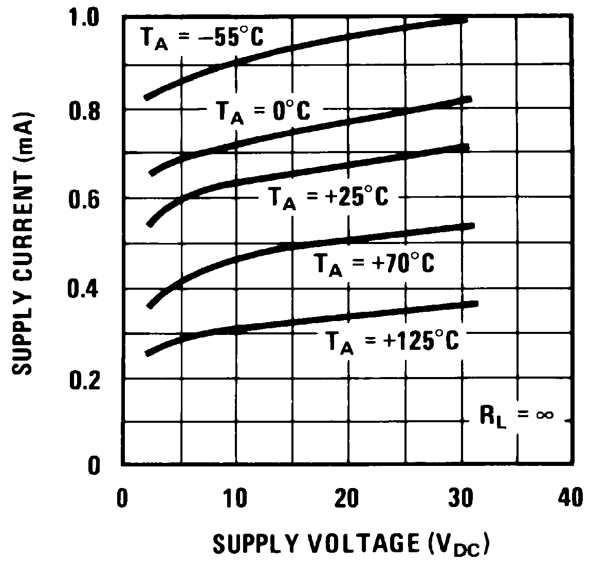 Figure 1. Supply Current
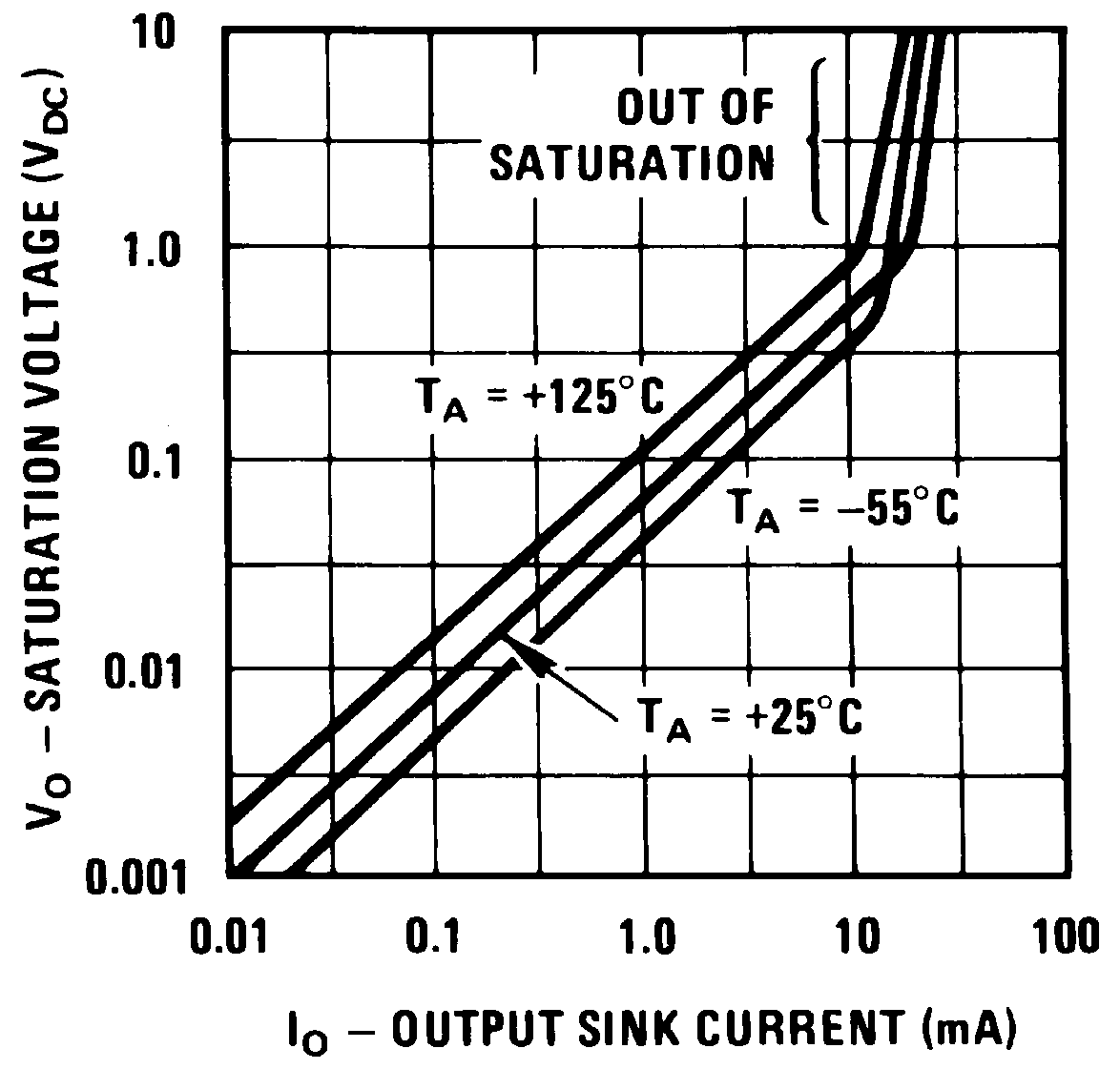 Figure 3. Output Saturation Voltage
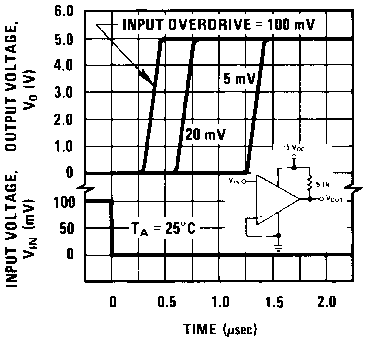 Figure 5. Response Time for Various Input Overdrives –
Positive Transition
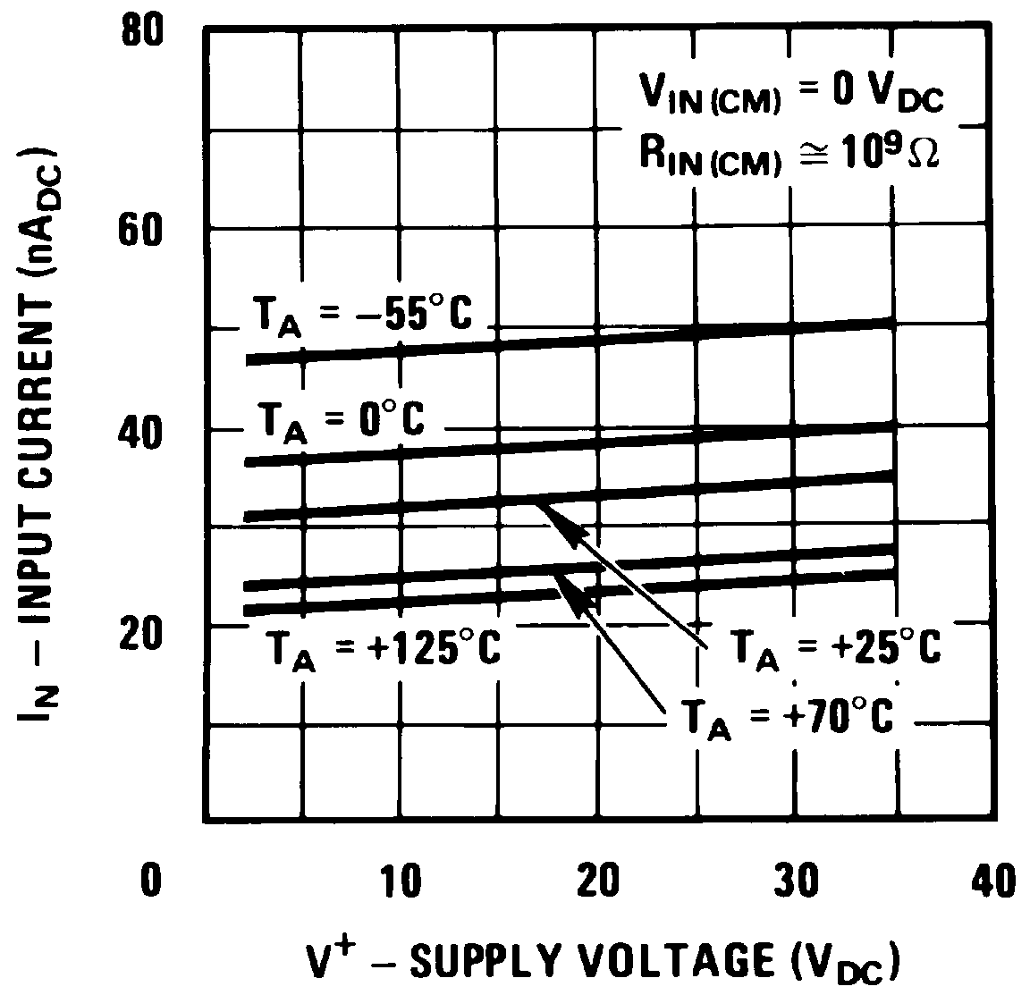 Figure 2. Input Current
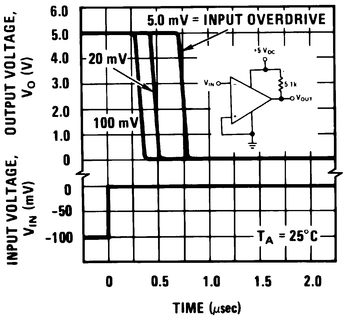 Figure 4. Response Time for Various Input Overdrives –
Negative Transition
6.7.2 LM2901
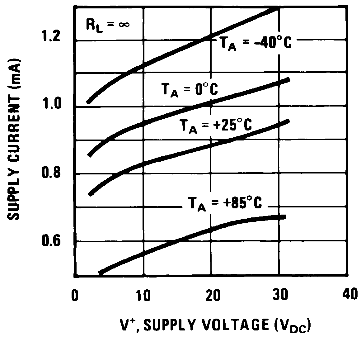 Figure 6. Supply Current
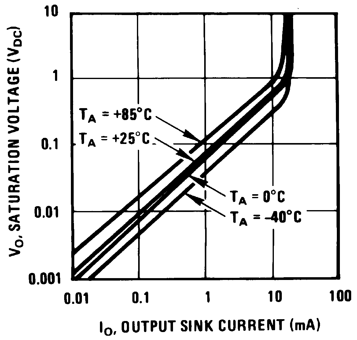 Figure 8. Output Saturation Voltage
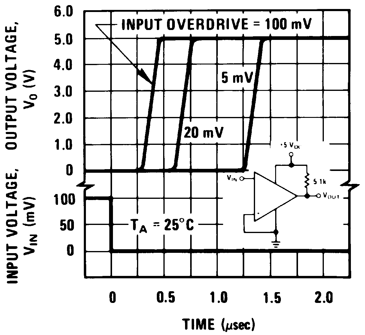 Figure 10. Response Time for Various Input Overdrives –
Positive Transition
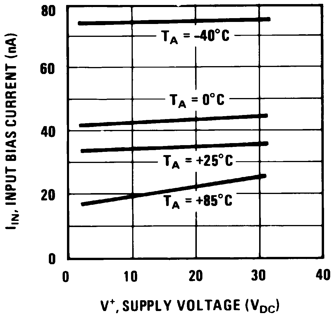 Figure 7. Input Current
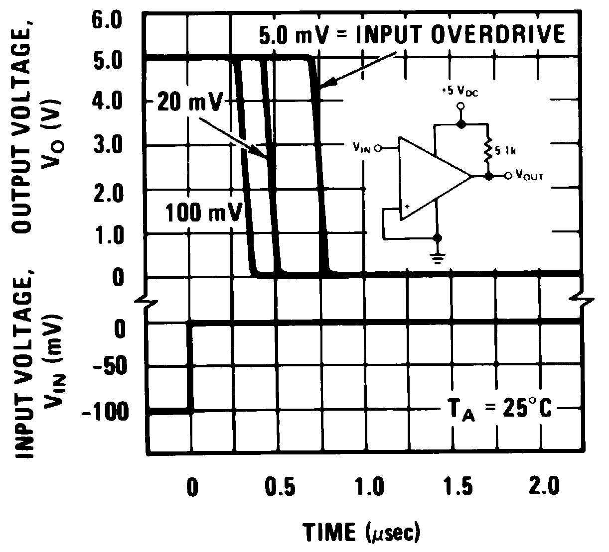 Figure 9. Response Time for Various Input Overdrives –
Negative Transition