SNIS161D March 2000 – January 2016 LM34
PRODUCTION DATA.
- 1 Features
- 2 Applications
- 3 Description
- 4 Revision History
- 5 Pin Configuration and Functions
- 6 Specifications
- 7 Detailed Description
- 8 Application and Implementation
- 9 Power Supply Recommendations
- 10Layout
- 11Device and Documentation Support
- 12Mechanical, Packaging, and Orderable Information
Package Options
Mechanical Data (Package|Pins)
Thermal pad, mechanical data (Package|Pins)
Orderable Information
7 Detailed Description
7.1 Overview
The LM34 series devices are precision integrated-circuit temperature sensors, whose output voltage is linearly proportional to the Fahrenheit temperature. The LM34 device has an advantage over linear temperature sensors calibrated in degrees Kelvin, because the user is not required to subtract a large constant voltage from its output to obtain convenient Fahrenheit scaling. The LM34 device does not require any external calibration or trimming to provide typical accuracies of ±1/2°F at room temperature and ±1-1⁄2°F over a full −50°F to 300°F temperature range. Lower cost is assured by trimming and calibration at the wafer level. The low output impedance, linear output, and precise inherent calibration of the LM34 device makes interfacing to readout or control circuitry especially easy. It can be used with single power supplies or with plus and minus supplies. Because the LM34 device draws only 75 µA from its supply, the device has very low self-heating, less than 0.2°F in still air.
The temperature sensing element is comprised of a simple base emitter junction that is forward biased by a current source. The temperature sensing element is buffered by an amplifier and provided to the OUT pin. The amplifier has a simple class-A output stage thus providing a low impedance output that can source 16 μA and sink 1 μA.
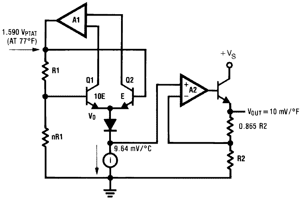
The temperature sensing element is comprised of a delta-VBE architecture. The temperature sensing element is then buffered by an amplifier and provided to the VOUT pin. The amplifier has a simple class A output stage with typical 0.5-Ω output impedance as shown in the Functional Block Diagram. Therefore, the LM34 device can only source current and the sinking capability of the device is limited to 1 µA.
7.2 Functional Block Diagram

7.3 Feature Description
7.3.1 Capacitive Drive Capability
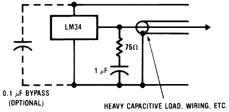
Like most micropower circuits, the LM34 device has a limited ability to drive heavy capacitive loads. The LM34 device, by itself, is able to drive 50 pF without special precautions. If heavier loads are anticipated, it is easy to isolate or decouple the load with a resistor; see Figure 12. You can improve the tolerance of capacitance with a series R-C damper from output to ground; see Figure 13. When the LM34 is applied with a 499-Ω load resistor (as shown Figure 18 and Figure 19), the device is relatively immune to wiring capacitance because the capacitance forms a bypass from ground to input, not on the output. However, as with any linear circuit connected to wires in a hostile environment, its performance can be affected adversely by intense electromagnetic sources such as relays, radio transmitters, motors with arcing brushes, transients of the SCR, and so on, as the wiring of the device can act as a receiving antenna and the internal junctions can act as rectifiers. For best results in such cases, a bypass capacitor from VIN to ground and a series R-C damper, such as 75 Ω in series with 0.2 μF or 1 μF from output to ground, are often useful. See Figure 23, Figure 24 and Figure 26 for more details.
 Figure 12. LM34 With Decoupling from Capacitive Load
 Figure 13. LM34 With R-C Damper
7.3.2 LM34 Transfer Function
The accuracy specifications of the LM34 devices are given with respect to a simple linear transfer function shown in Equation 1:
where
- VOUT is the LM34 output voltage
- T is the temperature in °F
7.4 Device Functional Modes
The only functional mode of the LM34 device is that it has an analog output directly proportional to temperature.