SNVS508D October 2007 – September 2016 LM3405A
PRODUCTION DATA.
- 1 Features
- 2 Applications
- 3 Description
- 4 Revision History
- 5 Pin Configuration and Functions
- 6 Specifications
- 7 Detailed Description
-
8 Application and Implementation
- 8.1 Application Information
- 8.2 Typical Applications
- 8.3
System Examples
- 8.3.1 VBOOST Derived from VOUT (VIN = 12 V, IF = 1 A)
- 8.3.2 VBOOST Derived from VIN through a Series Zener Diode (D3) (VIN = 15 V, IF = 1 A)
- 8.3.3 VBOOST Derived from VIN through a Shunt Zener Diode (D3) (VIN = 18 V, IF = 1 A)
- 8.3.4 LED MR16 Lamp Application (VIN = 12-V AC, IF = 0.75 A)
- 8.3.5 VBOOST Derived from VOUT through a Series Zener Diode (D3) ( VIN = 18 V, IF = 1 A )
- 9 Power Supply Recommendations
- 10Layout
- 11Device and Documentation Support
- 12Mechanical, Packaging, and Orderable Information
- 12Mechanical, Packaging, and Orderable Information
Package Options
Mechanical Data (Package|Pins)
Thermal pad, mechanical data (Package|Pins)
- DGN|8
Orderable Information
8 Application and Implementation
NOTE
Information in the following applications sections is not part of the TI component specification, and TI does not warrant its accuracy or completeness. TI’s customers are responsible for determining suitability of components for their purposes. Customers should validate and test their design implementation to confirm system functionality.
8.1 Application Information
8.1.1 Inductor (L1)
The Duty Cycle (D) can be approximated quickly using the ratio of output voltage (VOUT) to input voltage (VIN):

The catch diode (D1) forward voltage drop and the voltage drop across the internal NMOS must be included to calculate a more accurate duty cycle. Calculate D by using Equation 12:

VSW can be approximated by Equation 13:
The diode forward drop (VD1) can range from 0.3 V to 0.7 V depending on the quality of the diode. The lower VD1 is, the higher the operating efficiency of the converter.
The inductor value determines the output ripple current (ΔiL, as defined in Figure 11). Lower inductor values decrease the size of the inductor, but increases the output ripple current. An increase in the inductor value will decrease the output ripple current. The ratio of ripple current to LED current is optimized when it is set between 0.3 and 0.4 at 1A LED current. This ratio r is defined as:

One must also ensure that the minimum current limit (1.2 A) is not exceeded, so the peak current in the inductor must be calculated. The peak current (ILPK) in the inductor is calculated as:
When the designed maximum output current is reduced, the ratio r can be increased. At a current of 0.2 A, r can be made as high as 0.7. The ripple ratio can be increased at lighter loads because the net ripple is actually quite low, and if r remains constant the inductor value can be made quite large. An equation empirically developed for the maximum ripple ratio at any current below 2 A is:
Note that this is just a guideline.
The LM3405A operates at a high frequency allowing the use of ceramic output capacitors without compromising transient response. Ceramic capacitors allow higher inductor ripple without significantly increasing LED current ripple. See the output capacitor and feed-forward capacitor sections for more details on LED current ripple.
Now that the ripple current or ripple ratio is determined, the inductance is calculated by Equation 17:

where
- fSW is the switching frequency
- IF is the LED current
When selecting an inductor, make sure that it is capable of supporting the peak output current without saturating. Inductor saturation will result in a sudden reduction in inductance and prevent the regulator from operating correctly. Because of the operating frequency of the LM3405A, ferrite based inductors are preferred to minimize core losses. This presents little restriction since the variety of ferrite based inductors is huge. Lastly, inductors with lower series resistance (DCR) will provide better operating efficiency. For recommended inductor selection, refer to Circuit Examples and Recommended Inductance Range in Table 1.
Table 1. Recommended Inductance Range
| IF | INDUCTANCE RANGE AND INDUCTOR CURRENT RIPPLE | |||
|---|---|---|---|---|
| 1 A | 6.8 µH-15 µH | |||
| Inductance | 6.8 µH | 10 µH | 15 µH | |
| ΔiL / IF(1) | 51% | 36% | 24% | |
| 0.6 A | 10 µH-22 µH | |||
| Inductance | 10 µH | 15 µH | 22 µH | |
| ΔiL / IF(1) | 58% | 39% | 26% | |
| 0.2 A | 15 µH-27 µH | |||
| Inductance | 15 µH | 22 µH | 27 µH | |
| ΔiL / IF(1) | 116% | 79% | 65% | |
8.1.2 Input Capacitor (C1)
An input capacitor is necessary to ensure that VIN does not drop excessively during switching transients. The primary specifications of the input capacitor are capacitance, voltage rating, RMS current rating, and ESL (Equivalent Series Inductance). The input voltage rating is specifically stated by the capacitor manufacturer. Make sure to check any recommended deratings and also verify if there is any significant change in capacitance at the operating input voltage and the operating temperature. The input capacitor maximum RMS input current rating (IRMS-IN) must be greater than:

It can be shown from the above equation that maximum RMS capacitor current occurs when D = 0.5. Always calculate the RMS at the point where the duty cycle D, is closest to 0.5. The ESL of an input capacitor is usually determined by the effective cross sectional area of the current path. A large leaded capacitor will have high ESL and an 0805 ceramic chip capacitor will have very low ESL. At the operating frequency of the LM3405A, certain capacitors may have an ESL so large that the resulting inductive impedance (2πfL) will be higher than that required to provide stable operation. It is strongly recommended to use ceramic capacitors due to their low ESR and low ESL. A 10µF multilayer ceramic capacitor (MLCC) is a good choice for most applications. In cases where large capacitance is required, use surface mount capacitors such as Tantalum capacitors and place at least a 1µF ceramic capacitor close to the VIN pin. For MLCCs it is recommended to use X7R or X5R dielectrics. Consult capacitor manufacturer datasheet to see how rated capacitance varies over operating conditions.
8.1.3 Output Capacitor (C2)
The output capacitor is selected based upon the desired reduction in LED current ripple. A 1µF ceramic capacitor results in very low LED current ripple for most applications. Due to the high switching frequency, the 1µF capacitor alone (without feed-forward capacitor C4) can filter more than 90% of the inductor current ripple for most applications where the sum of LED dynamic resistance and R1 is larger than 1Ω. Since the internal compensation is tailored for small output capacitance with very low ESR, it is strongly recommended to use a ceramic capacitor with capacitance less than 3.3µF.
Given the availability and quality of MLCCs and the expected output voltage of designs using the LM3405A, there is really no need to review other capacitor technologies. A benefit of ceramic capacitors is their ability to bypass high frequency noise. A certain amount of switching edge noise will couple through the parasitic capacitances in the inductor to the output. A ceramic capacitor will bypass this noise. In cases where large capacitance is required, use Electrolytic or Tantalum capacitors with large ESR, and verify the loop performance on the bench. Like the input capacitor, multilayer ceramic capacitors are recommended X7R or X5R. Again, verify actual capacitance at the desired operating voltage and temperature.
Check the RMS current rating of the capacitor. The maximum RMS current rating of the capacitor is:

One may select a 1206 size ceramic capacitor for C2 since its current rating is typically higher than 1A, more than enough for the requirement.
8.1.4 Feed-Forward Capacitor (C4)
The feed-forward capacitor (designated as C4) connected in parallel with the LED string is required to provide multiple benefits to the LED driver design. It greatly improves the large signal transient response and suppresses LED current overshoot that may otherwise occur during PWM dimming; it also helps to shape the rise and fall times of the LED current pulse during PWM dimming thus reducing EMI emission; it reduces LED current ripple by bypassing some of inductor ripple from flowing through the LED. For most applications, a 1-µF ceramic capacitor is sufficient. In fact, the combination of a 1µF feed-forward ceramic capacitor and a 1µF output ceramic capacitor leads to less than 1% current ripple flowing through the LED. Lower and higher C4 values can be used, but bench validation is required to ensure the performance meets the application requirement.
Figure 21 shows a typical LED current waveform during PWM dimming without feed-forward capacitor. At the beginning of each PWM cycle, overshoot can be seen in the LED current. Adding a 1µF feed-forward capacitor can totally remove the overshoot as shown in Figure 22.
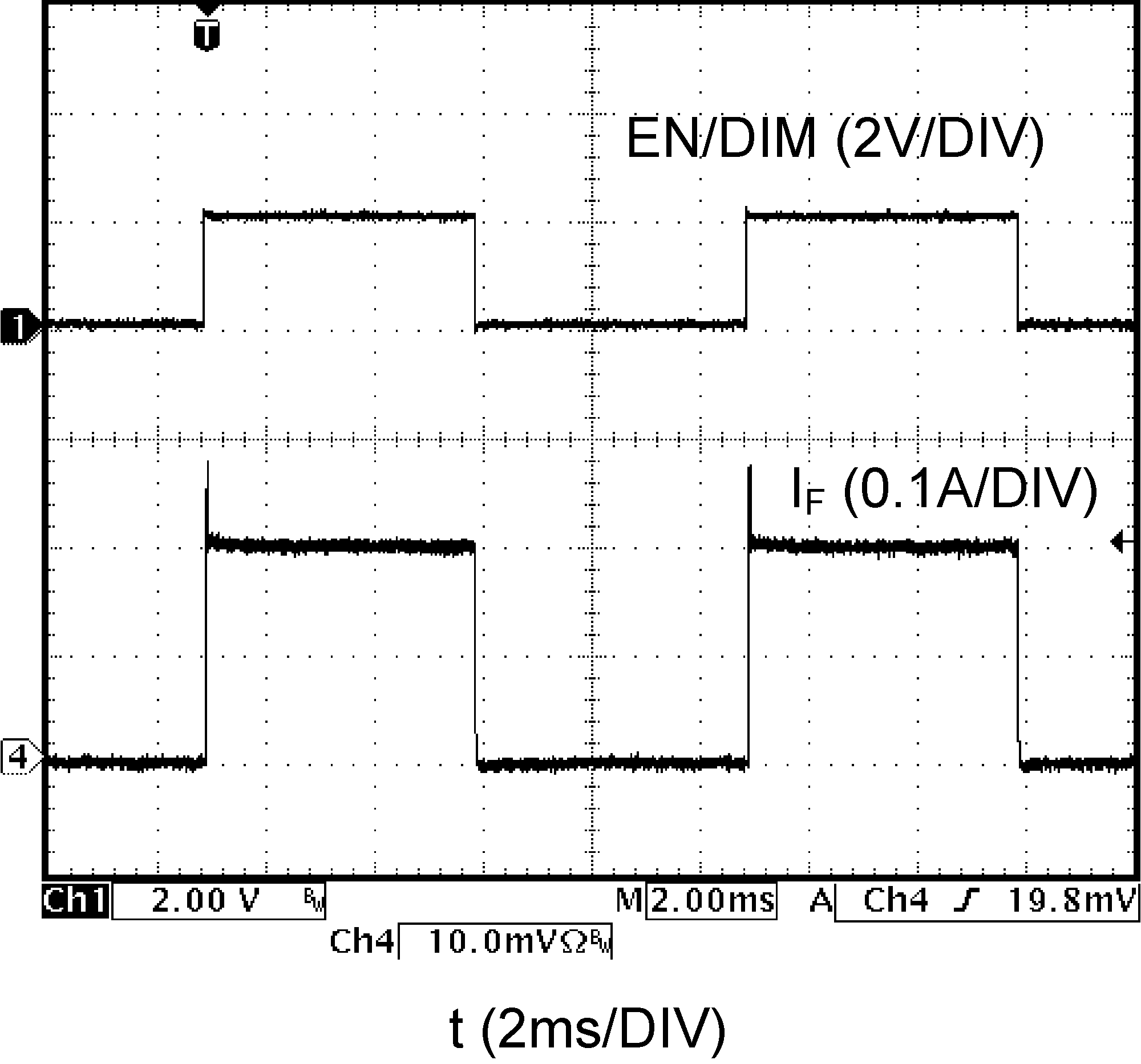 Figure 21. PWM Dimming Without Feed-Forward Capacitor
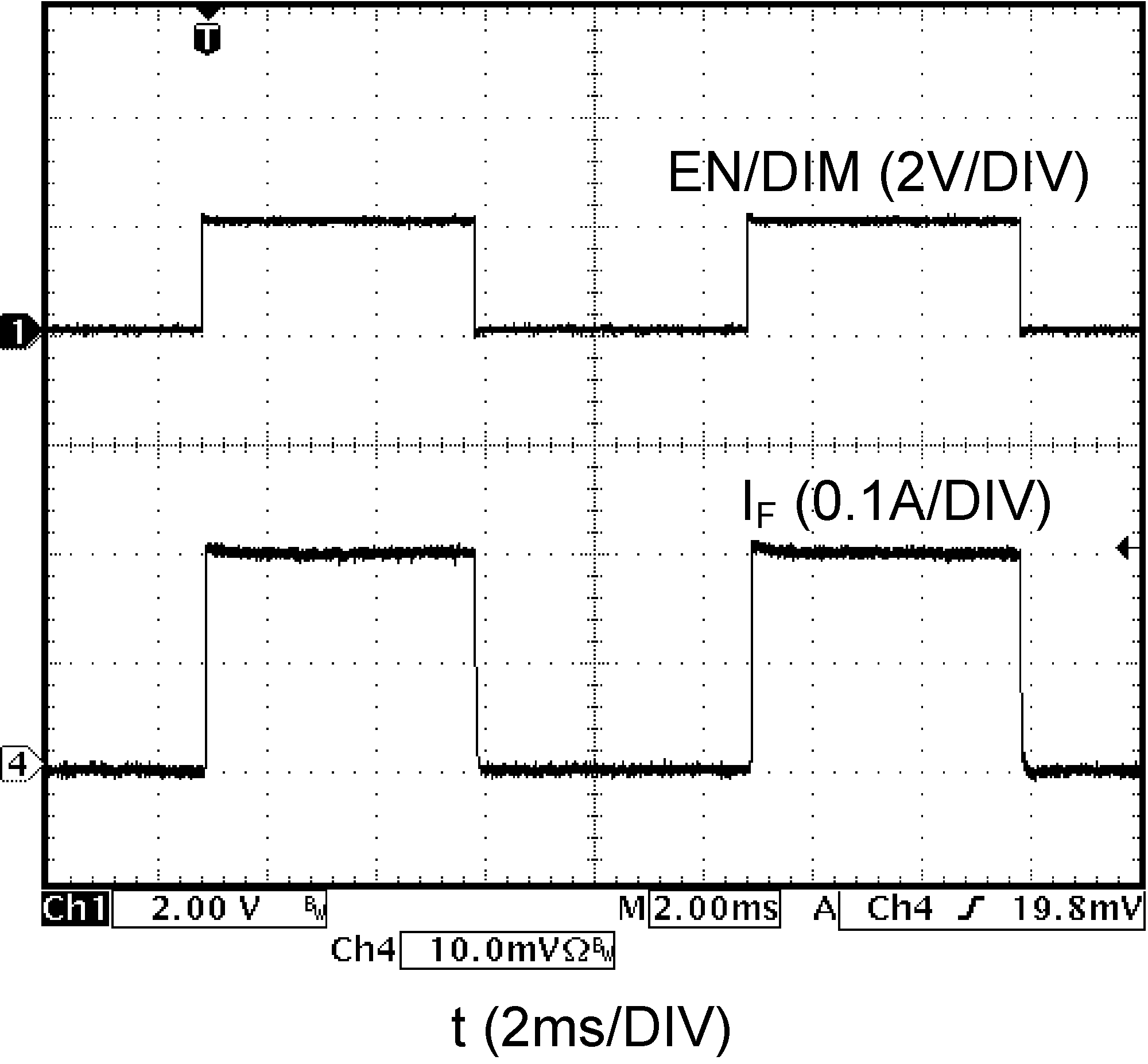 Figure 22. PWM Dimming With a 1-µF Feed-Forward Capacitor
8.1.5 Catch Diode (D1)
The catch diode (D1) conducts during the switch off-time. A Schottky diode is required for its fast switching time and low forward voltage drop. The catch diode should be chosen such that its current rating is greater than:
The reverse breakdown rating of the diode must be at least the maximum input voltage plus appropriate margin. To improve efficiency, choose a Schottky diode with a low forward voltage drop.
8.1.6 Boost Diode (D2)
A standard diode such as the 1N4148 type is recommended. For VBOOST circuits derived from voltages less than 3.3V, a small-signal Schottky diode is recommended for better efficiency. A good choice is the BAT54 small signal diode.
8.1.7 Boost Capacitor (C3)
A 0.01µF ceramic capacitor with a voltage rating of at least 6.3V is sufficient. The X7R and X5R MLCCs provide the best performance.
8.1.8 Power Loss Estimation
The main power loss in LM3405A includes three basic types of loss in the internal power switch: conduction loss, switching loss, and gate charge loss. In addition, there is loss associated with the power required for the internal circuitry of IC.
The conduction loss is calculated as:

If the inductor ripple current is fairly small (for example, less than 40%) , the conduction loss can be simplified to:
The switching loss occurs during the switch on and off transition periods, where voltage and current overlap resulting in power loss. The simplest means to determine this loss is to empirically measure the rise and fall times (10% to 90%) of the voltage at the switch pin.
Switching power loss is calculated as follows:
The gate charge loss is associated with the gate charge QG required to drive the switch:
The power loss required for operation of the internal circuitry:
IQ is the quiescent operating current, and is typically around 1.8mA for the LM3405A.
The total power loss in the IC is:
An example of power losses for a typical application is shown in Table 2:
Table 2. Power Loss Tabulation
| CONDITIONS | POWER LOSS | ||
|---|---|---|---|
| VIN | 12 V | ||
| VOUT | 3.9 V | ||
| IOUT | 1 A | ||
| VD1 | 0.45 V | ||
| RDS(ON) | 300 mΩ | PCOND | 108 mW |
| fSW | 1.6 MHz | ||
| TRISE | 18 ns | PSW | 288 mW |
| TFALL | 12 ns | ||
| IQ | 1.8 mA | PQ | 22 mW |
| QG | 1.4 nC | PG | 27 mW |
| D is calculated to be 0.36 | |||
8.2 Typical Applications
8.2.1 VBOOST Derived from VIN (VIN = 5 V, IF = 1 A)
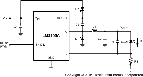 Figure 23. VBOOST Derived from VIN
(VIN = 5 V, IF = 1 A) Diagram
8.2.1.1 Design Requirements
- Input Voltage: VIN = 5 V ± 10%
- LED Current: IF = 1 A
- LED Forward Voltage: VLED = 3.4 V
- Output Voltage: VOUT = 3.4 V + 0.2 V = 3.6 V
- Ripple Ratio: r < 0.6
- PWM Dimmable
8.2.1.2 Detailed Design Procedure
8.2.1.2.1 Calculate Duty Cycle (D)
Calculate the nominal duty cycle for calculations and ensure the maximum duty cycle will not be exceeded in the application using Equation 29:

Using the same equation DMAX can be calculated for the minimum input voltage of 4.5 V. The duty cycle at 4.5 V is 0.8 which is less than the minimum DMAX of 0.85 specified in Electrical Characteristics.
8.2.1.2.2 Choose Capacitor Values (C1, C2, C3, and C4)
Low input voltage applications and PWM dimming applications generally require more input capacitance so the higher value of C1 = 10 µF is chosen for best performance. The other capacitor values chosen are the recommended values of C2 = C4 = 1 µF and C3 = 0.01 µF. All capacitors chosen are X5R or X7R dielectric ceramic capacitors of sufficient voltage rating.
8.2.1.2.3 Set the Nominal LED Current (R1)
The nominal LED current at 100% PWM dimming duty cycle is set by the resistor R1. R1 can be calculated using Equation 30:

The standard value of R1 = 0.2Ω is chosen. R1 should have a power rating of at least 1/4 W.
8.2.1.2.4 Choose Diodes (D1 and D2)
For the boost diode, D2, choose a low current diode with a voltage rating greater than the input voltage to give some margin. D2 should also be a schottky to minimize the forward voltage drop. For this example a schottky diode of D2 = 100 mA, 30 V is chosen. The catch diode, D1, should be a schottky diode and should have a voltage rating greater than the input voltage and a current rating greater than the average current. The average current in D1 can be calculated with Equation 31:

For this example D1 = 1 A, 10 V is chosen.
8.2.1.2.5 Calculate the Inductor Value (L1)
The inductor value is chosen for a given ripple ratio (r). To calculate L1 the forward voltage of D1 is required. In this case the chosen diode has a forward voltage drop of VF = 0.37 V. Given the desired ripple ratio L1 is calculated as:

The next larger standard value of L1 = 4.7 µH is chosen. A ripple ratio of 0.6 translates to a ΔiL of 600 mA and a peak inductor current of 1.3 A (IF + ΔiL/2). Choose an inductor with a saturation current rating of greater than
1.3 A.
Table 3. Bill of Materials for Figure 23
| PART ID | PART VALUE | PART NUMBER | MANUFACTURER |
|---|---|---|---|
| U1 | 1-A LED Driver | LM3405A | Texas Instruments |
| C1, Input Cap | 10 µF, 6.3 V, X5R | C3216X5R0J106M | TDK |
| C2, Output Cap | 1 µF, 10 V, X7R | GRM319R71A105KC01D | Murata |
| C3, Boost Cap | 0.01 µF, 16 V, X7R | 0805YC103KAT2A | AVX |
| C4, Feedforward Cap | 1 µF, 10 V, X7R | GRM319R71A105KC01D | Murata |
| D1, Catch Diode | Schottky, 0.37 V at 1A, VR = 10 V | MBRM110LT1G | ON Semiconductor |
| D2, Boost Diode | Schottky, 0.36 V at 15 mA | CMDSH-3 | Central Semiconductor |
| L1 | 4.7 µH, 1.6 A | SLF6028T-4R7M1R6 | TDK |
| R1 | 0.2 Ω, 0.5 W, 1% | WSL2010R2000FEA | Vishay |
| LED1 | 1.5 A, White LED | LXK2-PW14 | Lumileds |
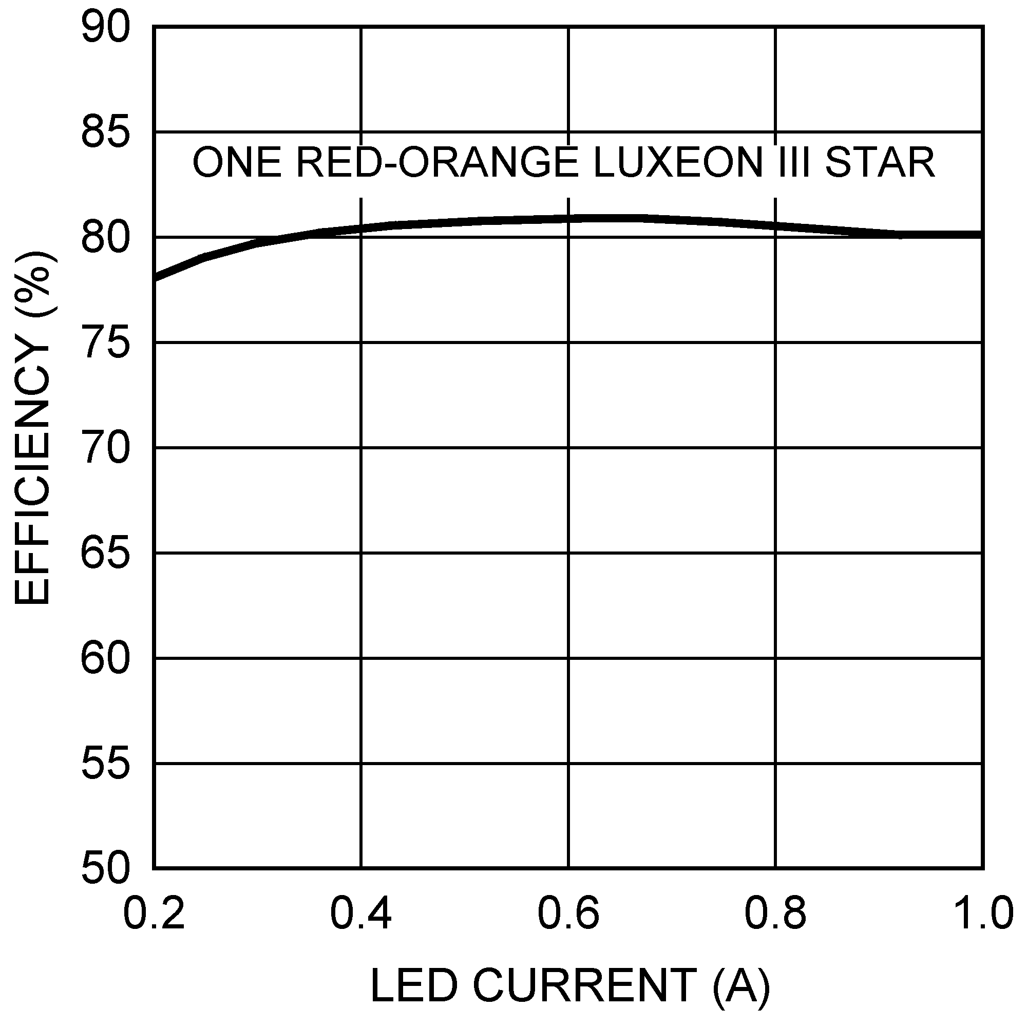
8.2.1.3 Application Curve
8.3 System Examples
8.3.1 VBOOST Derived from VOUT (VIN = 12 V, IF = 1 A)
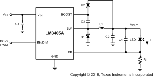 Figure 25. VBOOST Derived from VOUT
(VIN = 12 V, IF = 1 A) Diagram
Table 4. Bill of Materials for Figure 25
| PART ID | PART VALUE | PART NUMBER | MANUFACTURER |
|---|---|---|---|
| U1 | 1-A LED Driver | LM3405A | Texas Instruments |
| C1, Input Cap | 10 µF, 25 V, X5R | ECJ-3YB1E106K | Panasonic |
| C2, Output Cap | 1 µF, 10 V, X7R | GRM319R71A105KC01D | Murata |
| C3, Boost Cap | 0.01 µF, 16 V, X7R | 0805YC103KAT2A | AVX |
| C4, Feedforward Cap | 1 µF, 10 V, X7R | GRM319R71A105KC01D | Murata |
| D1, Catch Diode | Schottky, 0.5 V at 1 A, VR = 30 V | SS13 | Vishay |
| D2, Boost Diode | Schottky, 0.36 V at 15 mA | CMDSH-3 | Central Semiconductor |
| L1 | 4.7 µH, 1.6 A | SLF6028T-4R7M1R6 | TDK |
| R1 | 0.2 Ω, 0.5 W, 1% | WSL2010R2000FEA | Vishay |
| LED1 | 1.5 A, White LED | LXK2-PW14 | Lumileds |
8.3.2 VBOOST Derived from VIN through a Series Zener Diode (D3) (VIN = 15 V, IF = 1 A)
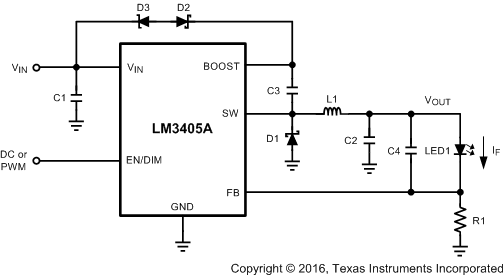 Figure 26. VBOOST Derived from VIN through a Series Zener Diode (D3)
(VIN = 15 V, IF = 1 A) Diagram
Table 5. Bill of Materials for Figure 26
| PART ID | PART VALUE | PART NUMBER | MANUFACTURER |
|---|---|---|---|
| U1 | 1-A LED Driver | LM3405A | Texas Instruments |
| C1, Input Cap | 10 µF, 25 V, X5R | ECJ-3YB1E106K | Panasonic |
| C2, Output Cap | 1 µF, 10 V, X7R | GRM319R71A105KC01D | Murata |
| C3, Boost Cap | 0.01 µF, 16 V, X7R | 0805YC103KAT2A | AVX |
| C4, Feedforward Cap | 1 µF, 10 V, X7R | GRM319R71A105KC01D | Murata |
| D1, Catch Diode | Schottky, 0.5 V at 1A, VR = 30 V | SS13 | Vishay |
| D2, Boost Diode | Schottky, 0.36 V at 15 mA | CMDSH-3 | Central Semiconductor |
| D3, Zener Diode | 11 V, 350 mW, SOT-23 | BZX84C11 | Fairchild |
| L1 | 6.8 µH, 1.5 A | SLF6028T-6R8M1R5 | TDK |
| R1 | 0.2 Ω, 0.5 W, 1% | WSL2010R2000FEA | Vishay |
| LED1 | 1.5 A, White LED | LXK2-PW14 | Lumileds |
8.3.3 VBOOST Derived from VIN through a Shunt Zener Diode (D3) (VIN = 18 V, IF = 1 A)
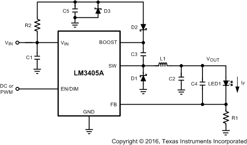 Figure 27. VBOOST Derived From VIN Through a Shunt Zener Diode (D3)
(VIN = 18 V, IF = 1 A) Diagram
Table 6. Bill of Materials for Figure 27
| PART ID | PART VALUE | PART NUMBER | MANUFACTURER |
|---|---|---|---|
| U1 | 1-A LED Driver | LM3405A | Texas Instruments |
| C1, Input Cap | 10 µF, 25 V, X5R | ECJ-3YB1E106K | Panasonic |
| C2, Output Cap | 1 µF, 10 V, X7R | GRM319R71A105KC01D | Murata |
| C3, Boost Cap | 0.01 µF, 16 V, X7R | 0805YC103KAT2A | AVX |
| C4, Feedforward Cap | 1 µF, 10 V, X7R | GRM319R71A105KC01D | Murata |
| C5, Shunt Cap | 0.1 µF, 16 V, X7R | GRM219R71C104KA01D | Murata |
| D1, Catch Diode | Schottky, 0.5 V at 1 A, VR = 30 V | SS13 | Vishay |
| D2, Boost Diode | Schottky, 0.36 V at 15 mA | CMDSH-3 | Central Semiconductor |
| D3, Zener Diode | 4.7 V, 35 0mW, SOT-23 | BZX84C4 V7 | Fairchild |
| L1 | 6.8 µH, 1.5 A | SLF6028T-6R8M1R5 | TDK |
| R1 | 0.2 Ω, 0.5 W, 1% | WSL2010R2000FEA | Vishay |
| R2 | 1.91 kΩ, 1% | CRCW08051K91FKEA | Vishay |
| LED1 | 1.5 A, White LED | LXK2-PW14 | Lumileds |
8.3.4 LED MR16 Lamp Application (VIN = 12-V AC, IF = 0.75 A)
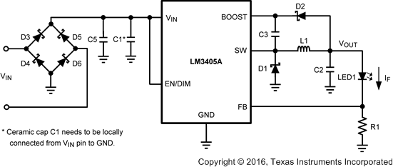 Figure 28. LED MR16 Lamp Application
(VIN = 12-V AC, IF = 0.75 A) Diagram
Table 7. Bill of Materials for Figure 28
8.3.5 VBOOST Derived from VOUT through a Series Zener Diode (D3) ( VIN = 18 V, IF = 1 A )
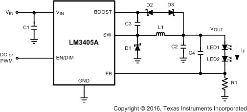 Figure 29. VBOOST Derived from VOUT Through a Series Zener Diode (D3)
( VIN = 18 V, IF = 1 A) Diagram
Table 8. Bill of Materials for Figure 29
| PART ID | PART VALUE | PART NUMBER | MANUFACTURER |
|---|---|---|---|
| U1 | 1-A LED Driver | LM3405A | Texas Instruments |
| C1, Input Cap | 10 µF, 25 V, X5R | ECJ-3YB1E106K | Panasonic |
| C2, Output Cap | 1 µF, 16 V, X7R | GRM319R71A105KC01D | Murata |
| C3, Boost Cap | 0.01 µF, 16 V, X7R | 0805YC103KAT2A | AVX |
| C4, Feedforward Cap | 1 µF, 16 V, X7R | GRM319R71A105KC01D | Murata |
| D1, Catch Diode | Schottky, 0.5 V at 1 A, VR = 30 V | SS13 | Vishay |
| D2, Boost Diode | Schottky, 0.36 V at 15 mA | CMDSH-3 | Central Semiconductor |
| D3, Zener Diode | 3.6 V, 350 mW, SOT-23 | BZX84C3V6 | Fairchild |
| L1 | 6.8 µH, 1.5 A | SLF6028T-6R8M1R5 | TDK |
| R1 | 0.2 Ω, 0.5 W, 1% | WSL2010R2000FEA | Vishay |
| LED1 | 1.5 A, White LED | LXK2-PW14 | Lumileds |
| LED2 | 1.5 A, White LED | LXK2-PW14 | Lumileds |