SNVS508D October 2007 – September 2016 LM3405A
PRODUCTION DATA.
- 1 Features
- 2 Applications
- 3 Description
- 4 Revision History
- 5 Pin Configuration and Functions
- 6 Specifications
- 7 Detailed Description
-
8 Application and Implementation
- 8.1 Application Information
- 8.2 Typical Applications
- 8.3
System Examples
- 8.3.1 VBOOST Derived from VOUT (VIN = 12 V, IF = 1 A)
- 8.3.2 VBOOST Derived from VIN through a Series Zener Diode (D3) (VIN = 15 V, IF = 1 A)
- 8.3.3 VBOOST Derived from VIN through a Shunt Zener Diode (D3) (VIN = 18 V, IF = 1 A)
- 8.3.4 LED MR16 Lamp Application (VIN = 12-V AC, IF = 0.75 A)
- 8.3.5 VBOOST Derived from VOUT through a Series Zener Diode (D3) ( VIN = 18 V, IF = 1 A )
- 9 Power Supply Recommendations
- 10Layout
- 11Device and Documentation Support
- 12Mechanical, Packaging, and Orderable Information
- 12Mechanical, Packaging, and Orderable Information
Package Options
Mechanical Data (Package|Pins)
Thermal pad, mechanical data (Package|Pins)
- DGN|8
Orderable Information
7 Detailed Description
7.1 Overview
The LM3405A is a PWM, current-mode controlled buck switching regulator designed to provide a simple, high efficiency solution for driving LEDs with a preset switching frequency of 1.6MHz. This high frequency allows the LM3405A to operate with small surface mount capacitors and inductors, resulting in LED drivers that need only a minimum amount of board space. The LM3405A is internally compensated, simple to use, and requires few external components.
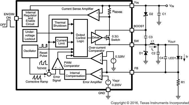
The following description of operation of the LM3405A refers to the Typical Application Circuit and to the waveforms in Figure 11. The LM3405A supplies a regulated output current by switching the internal NMOS power switch at constant frequency and variable duty cycle. A switching cycle begins at the falling edge of the reset pulse generated by the internal oscillator. When this pulse goes low, the output control logic turns on the internal NMOS power switch. During this on-time, the SW pin voltage (VSW) swings up to approximately VIN, and the inductor current (IL) increases with a linear slope. IL is measured by the current sense amplifier, which generates an output proportional to the switch current. The sense signal is summed with the regulator’s corrective ramp and compared to the error amplifier’s output, which is proportional to the difference between the feedback voltage and VREF. When the PWM comparator output goes high, the internal power switch turns off until the next switching cycle begins. During the switch off-time, inductor current discharges through the catch diode D1, which forces the SW pin to swing below ground by the forward voltage (VD1) of the catch diode. The regulator loop adjusts the duty cycle (D) to maintain a constant output current (IF) through the LED, by forcing FB pin voltage to be equal to VREF (0.205 V).
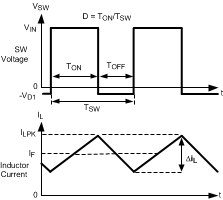 Figure 11. SW Pin Voltage and Inductor Current Waveforms of LM3405A
7.2 Functional Block Diagram
7.3 Feature Description
7.3.1 Boost Function
Capacitor C3 and diode D2 in the Functional Block Diagram are used to generate a voltage VBOOST. The voltage across C3, VBOOST - VSW, is the gate drive voltage to the internal NMOS power switch. To properly drive the internal NMOS switch during its on-time, VBOOST needs to be at least 2.5-V greater than VSW. A large value of VBOOST - VSW is recommended to achieve better efficiency by minimizing both the internal switch ON resistance (RDS(ON)), and the switch rise and fall times. However, VBOOST - VSW should not exceed the maximum operating limit of 5.5 V.
When the LM3405A starts up, internal circuitry from VIN supplies a 20-mA current to the BOOST pin, flowing out of the BOOST pin into C3. This current charges C3 to a voltage sufficient to turn the switch on. The BOOST pin will continue to source current to C3 until the voltage at the feedback pin is greater than 123 mV.
There are various methods to derive VBOOST:
- From the input voltage (VIN)
- From the output voltage (VOUT)
- From a shunt or series Zener diode
- From an external distributed voltage rail (VEXT)
The first method is shown in the Functional Block Diagram. Capacitor C3 is charged via diode D2 by VIN. During a normal switching cycle, when the internal NMOS power switch is off (TOFF) (see Figure 11), VBOOST equals VIN minus the forward voltage of D2 (VD2), during which the current in the inductor (L1) forward biases the catch diode D1 (VD1). Therefore the gate drive voltage stored across C3 is:
When the NMOS switch turns on (TON), the switch pin rises to:
Since the voltage across C3 remains unchanged, VBOOST is forced to rise thus reverse biasing D2. The voltage at VBOOST is then:
Depending on the quality of the diodes D1 and D2, the gate drive voltage in this method can be slightly less or larger than the input voltage VIN. For best performance, ensure that the variation of the input supply does not cause the gate drive voltage to fall outside the recommended range:
The second method for deriving the boost voltage is to connect D2 to the output as shown in Figure 12. The gate drive voltage in this configuration is:
Since the gate drive voltage needs to be in the range of 2.5 V to 5.5 V, the output voltage VOUT should be limited to a certain range. For the calculation of VOUT, see Output Voltage.
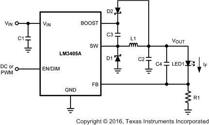 Figure 12. VBOOST Derived from VOUT
The third method can be used in the applications where both VIN and VOUT are greater than 5.5 V. In these cases, C3 cannot be charged directly from these voltages; instead C3 can be charged from VIN or VOUT minus a Zener voltage (VD3) by placing a Zener diode D3 in series with D2 as shown in Figure 13. When using a series Zener diode from the input, the gate drive voltage is VIN - VD3 - VD2 + VD1.
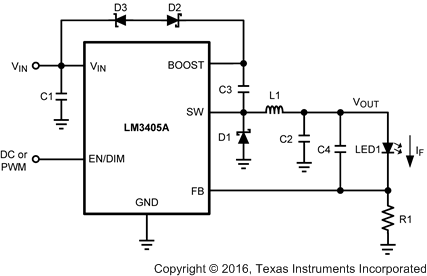 Figure 13. VBOOST Derived from VIN Through a Series Zener
An alternate method is to place the zener diode D3 in a shunt configuration as shown in Figure 14. A small 350 mW to 500 mW, 5.1-V Zener in a SOT or SOD package can be used for this purpose. A small ceramic capacitor such as a 6.3 V, 0.1-µF capacitor (C5) should be placed in parallel with the Zener diode. When the internal NMOS switch turns on, a pulse of current is drawn to charge the internal NMOS gate capacitance. The 0.1-µF parallel shunt capacitor ensures that the VBOOST voltage is maintained during this time. Resistor R2 should be chosen to provide enough RMS current to the zener diode and to the BOOST pin. A recommended choice for the zener current (IZENER) is 1 mA. The current IBOOST into the BOOST pin supplies the gate current of the NMOS power switch. It reaches a maximum of around 3.6 mA at the highest gate drive voltage of 5.5 V over the LM3405A operating range.
For the worst case IBOOST, increase the current by 50%. In that case, the maximum boost current will be:
R2 will then be given by:
For example, let VIN = 12 V, VZENER = 5V, IZENER = 1 mA, then:
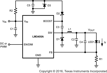 Figure 14. VBOOST Derived from VIN Through a Shunt Zener
The fourth method can be used in an application which has an external low voltage rail, VEXT. C3 can be charged through D2 from VEXT, independent of VIN and VOUT voltage levels. Again for best performance, ensure that the gate drive voltage, VEXT - VD2 + VD1, falls in the range of 2.5 V to 5.5 V.
7.3.2 Setting the LED Current
LM3405A is a constant current buck regulator. The LEDs are connected between VOUT and the FB pin as shown in the Typical Application Circuit. The FB pin is at 0.205V in regulation and therefore the LED current IF is set by VFB and resistor R1 from FB to ground by the following equation:
IF should not exceed the 1-A current capability of LM3405A and therefore R1 minimum must be approximately 0.2 Ω. IF should also be kept above 200 mA for stable operation, and therefore R1 maximum must be approximately 1 Ω. If average LED currents less than 200 mA are desired, the EN/DIM pin can be used for PWM dimming. See LED PWM Dimming.
7.3.3 Output Voltage
The output voltage is primarily determined by the number of LEDs (n) connected from VOUT to FB pin and therefore VOUT can be written as:
where
- VF is the forward voltage of one LED at the set LED current level (see LED manufacturer data sheet for forward characteristics curve)
7.3.4 Enable Mode / Shutdown Mode
The LM3405A has both enable and shutdown modes that are controlled by the EN/DIM pin. Connecting a voltage source greater than 1.8 V to the EN/DIM pin enables the operation of LM3405A, while reducing this voltage below 0.4 V places the part in a low quiescent current (0.3 µA typical) shutdown mode. There is no internal pullup on EN/DIM pin, therefore an external signal is required to initiate switching. Do not allow this pin to float or rise to 0.3 V above VIN. It should be noted that when the EN/DIM pin voltage rises above 1.8 V while the input voltage is greater than UVLO, there is a finite delay before switching starts. During this delay the LM3405A will go through a power on reset state after which the internal soft-start process commences. The soft-start process limits the inrush current and brings up the LED current (IF) in a smooth and controlled fashion. The total combined duration of the power on reset delay, soft-start delay and the delay to fully establish the LED current is in the order of 100 µs (see Figure 19).
The simplest way to enable the operation of LM3405A is to connect the EN/DIM pin to VIN which allows self start-up of LM3405A whenever the input voltage is applied. However, when an input voltage of slow rise time is used to power the application and if both the input voltage and the output voltage are not fully established before the soft-start time elapses, the control circuit will command maximum duty cycle operation of the internal power switch to bring up the output voltage rapidly. When the feedback pin voltage exceeds 0.205 V, the duty cycle will have to reduce from the maximum value accordingly, to maintain regulation. It takes a finite amount of time for this reduction of duty cycle and this will result in a spike in LED current for a short duration as shown in Figure 15. In applications where this LED current overshoot is undesirable, EN/DIM pin voltage can be separately applied and delayed such that VIN is fully established before the EN/DIM pin voltage reaches the enable threshold. The effect of delaying EN/DIM with respect to VIN on the LED current is shown in Figure 16. For a fast rising input voltage (200 µs for example), there is no need to delay the EN/DIM signal since soft-start can smoothly bring up the LED current as shown in Figure 17.
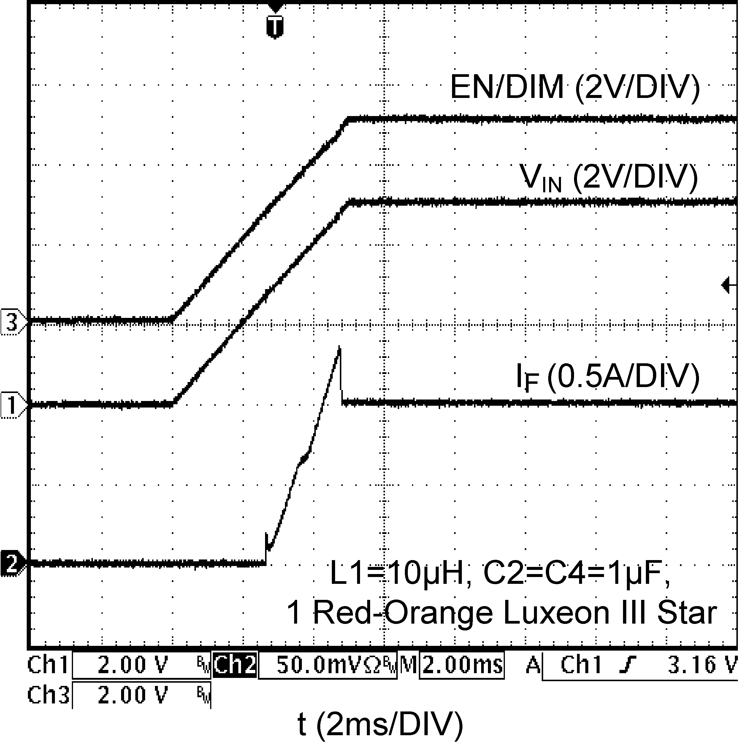 Figure 15. Start-Up Response to VIN With 5-ms Rise Time
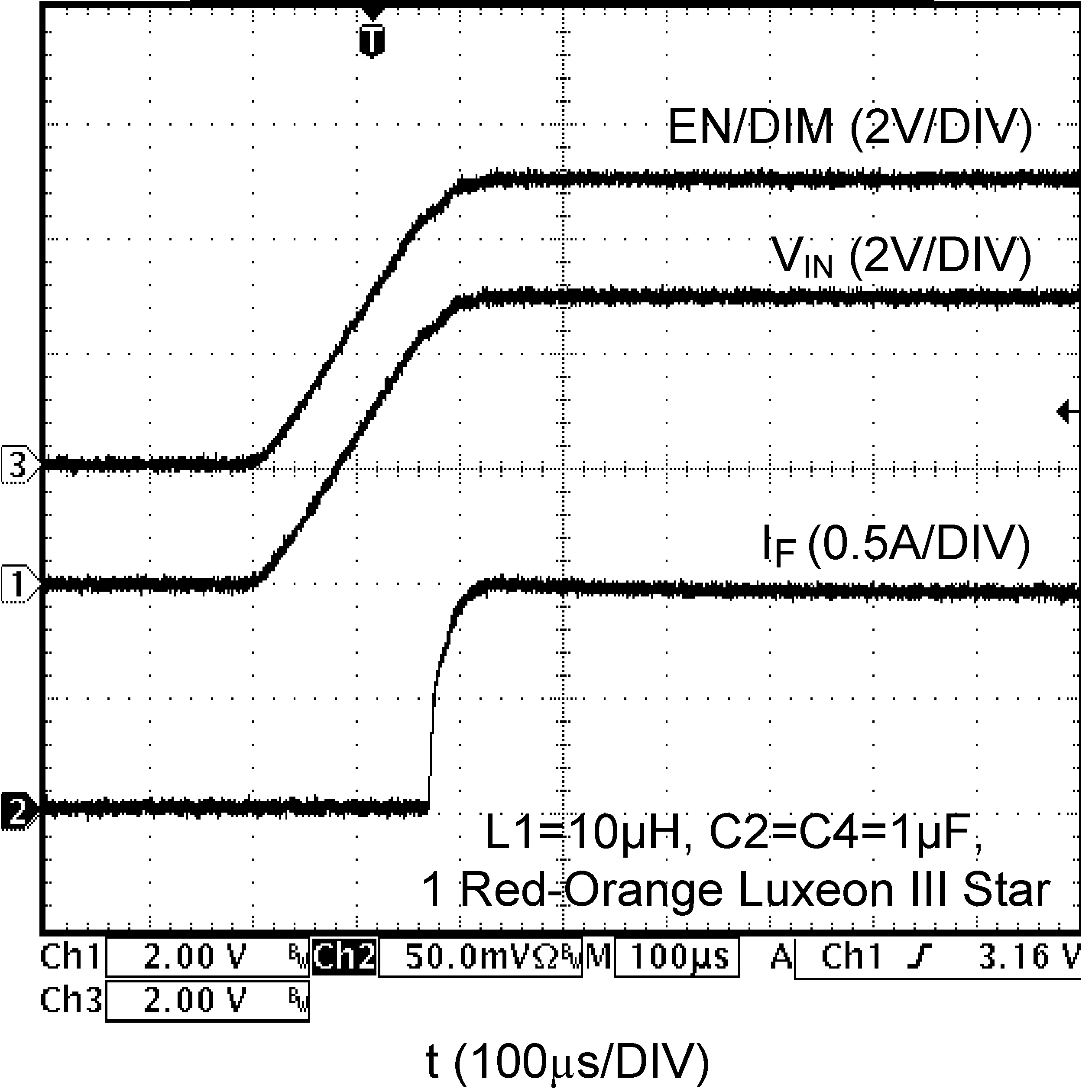 Figure 17. Start-Up Response to VIN With 200-µs Rise Time
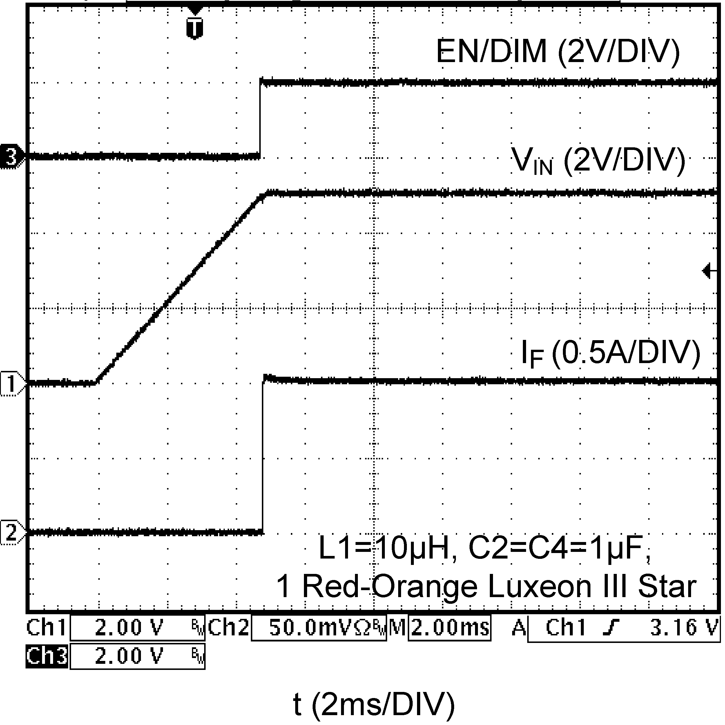 Figure 16. Start-Up Response to VIN With EN/DIM Delayed
7.3.5 LED PWM Dimming
The LED brightness can be controlled by applying a periodic pulse signal to the EN/DIM pin and varying its frequency and/or duty cycle. This so-called PWM dimming method controls the average light output by pulsing the LED current between the set value and zero. A logic high level at the EN/DIM pin turns on the LED current whereas a logic low level turns off the LED current. Figure 18 shows a typical LED current waveform in PWM dimming mode. As explained in the previous section, there is approximately a 100-µs delay from the EN/DIM signal going high to fully establishing the LED current as shown in Figure 19. This 100-µs delay sets a maximum frequency limit for the driving signal that can be applied to the EN/DIM pin for PWM dimming. Figure 20 shows the average LED current versus duty cycle of PWM dimming signal for various frequencies. The applicable frequency range to drive LM3405A for PWM dimming is from 100 Hz to 5 kHz. The dimming ratio reduces drastically when the applied PWM dimming frequency is greater than 5 kHz.
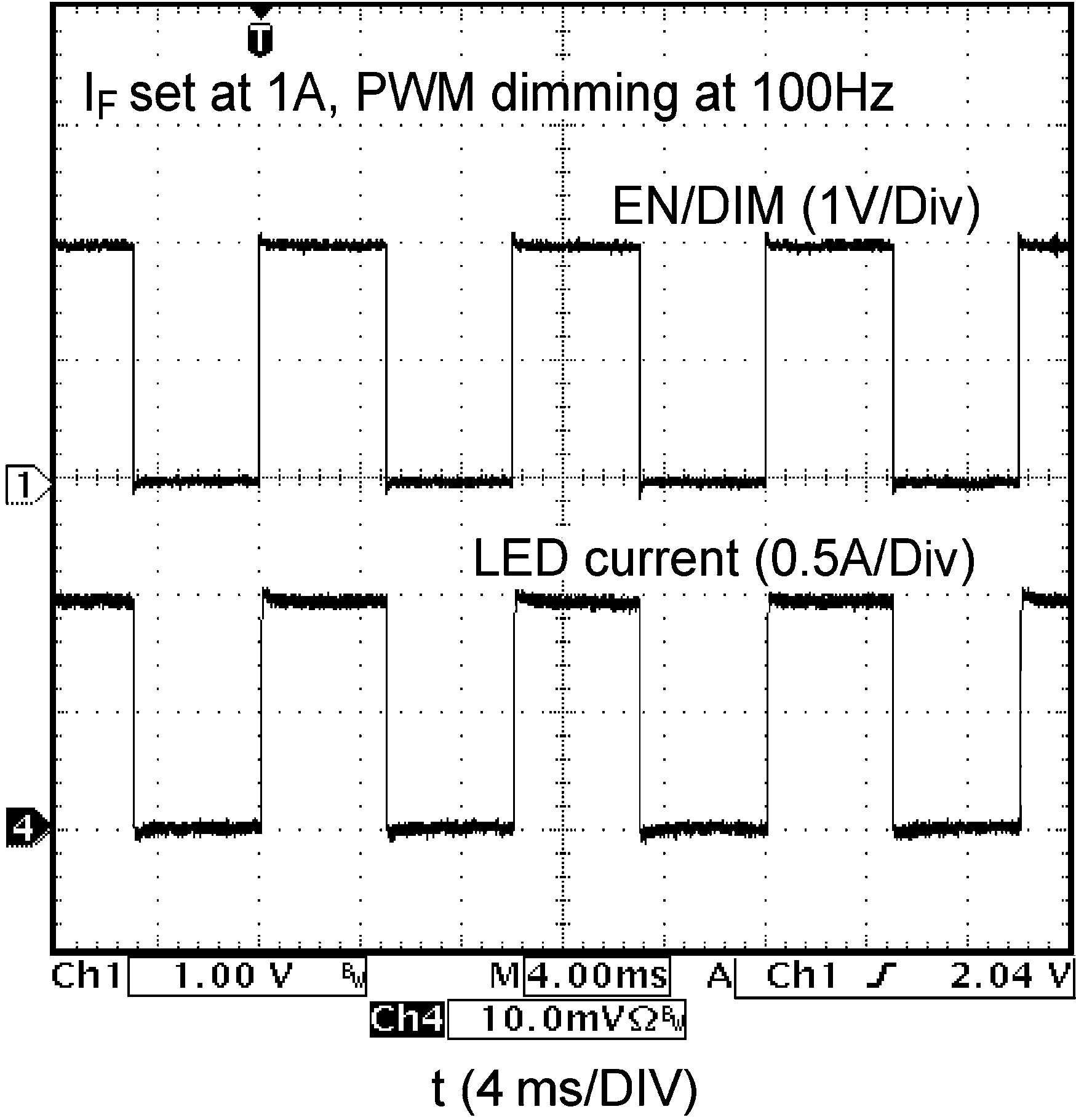 Figure 18. PWM Dimming of LEDs
Using the EN/DIM Pin
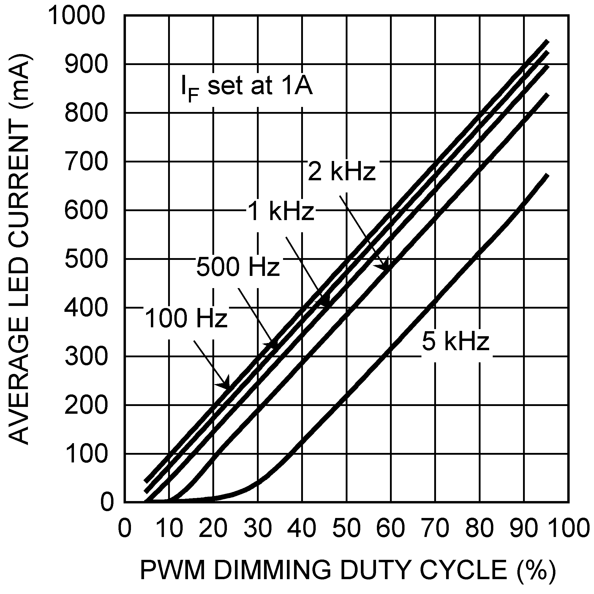 Figure 20. Average LED Current vs
Duty Cycle of PWM Dimming Signal at EN/DIM Pin
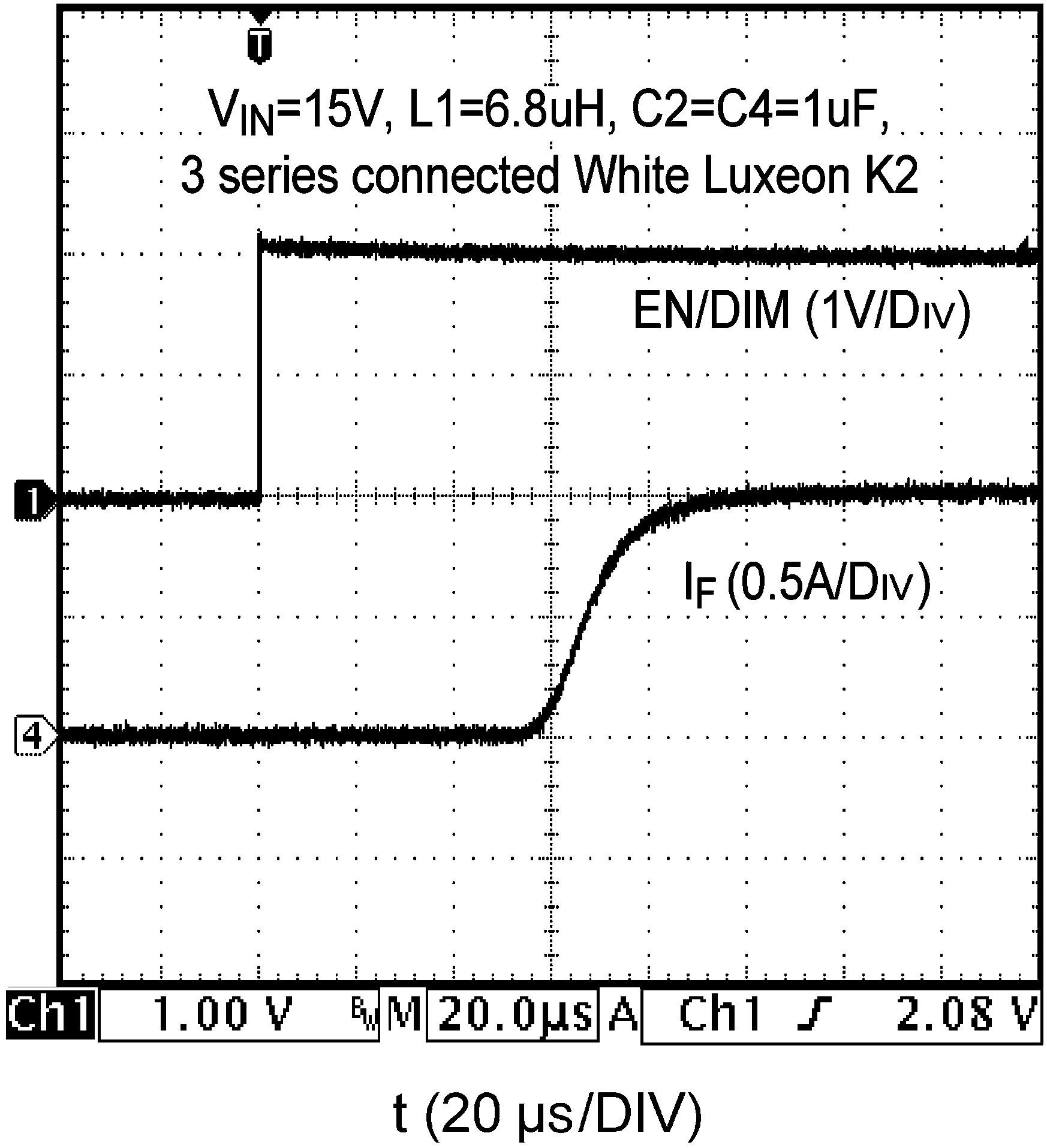 Figure 19. Start-Up Response to EN/DIM
With IF = 1 A
7.3.6 Undervoltage Lockout
Undervoltage lockout (UVLO) prevents the LM3405A from operating until the input voltage exceeds 2.74 V (typical). The UVLO threshold has approximately 440 mV of hysteresis, so the part will operate until VIN drops below 2.3 V (typical). Hysteresis prevents the part from turning off during power up if VIN is non-monotonic.
7.3.7 Current Limit
The LM3405A uses cycle-by-cycle current limit to protect the internal power switch. During each switching cycle, a current limit comparator detects if the power switch current exceeds 2 A (typical), and turns off the switch until the next switching cycle begins.
7.3.8 Overcurrent Protection
The LM3405A has a built-in overcurrent comparator that compares the FB pin voltage to a threshold voltage that is 60% higher than the internal reference VREF. Once the FB pin voltage exceeds this threshold level (typically 328 mV), the internal NMOS power switch is turned off, which allows the feedback voltage to decrease towards regulation. This threshold provides an upper limit for the LED current. LED current overshoot is limited to 328 mV/R1 by this comparator during transients.
7.4 Device Functional Modes
7.4.1 Thermal Shutdown
Thermal shutdown limits total power dissipation by turning off the internal power switch when the IC junction temperature exceeds 165°C. After thermal shutdown occurs, the power switch does not turn on until the junction temperature drops below approximately 150°C.