SNVS602L March 2009 – June 2016 LM3409 , LM3409-Q1 , LM3409HV , LM3409HV-Q1
PRODUCTION DATA.
- 1 Features
- 2 Applications
- 3 Description
- 4 Revision History
- 5 Device Comparison Table
- 6 Pin Configuration and Functions
- 7 Specifications
-
8 Detailed Description
- 8.1 Overview
- 8.2 Functional Block Diagram
- 8.3 Feature Description
- 8.4 Device Functional Modes
-
9 Application and Implementation
- 9.1
Application Information
- 9.1.1 Input Undervoltage Lockout (UVLO)
- 9.1.2 Operation Near Dropout
- 9.1.3 LED Ripple Current
- 9.1.4 Buck Converters without Output Capacitors
- 9.1.5 Buck Converters With Output Capacitors
- 9.1.6 Output Overvoltage Protection
- 9.1.7 Input Capacitors
- 9.1.8 P-Channel MOSFET (PFET)
- 9.1.9 Re-Circulating Diode
- 9.2
Typical Applications
- 9.2.1 EN PIN PWM Dimming Application for 10 LEDs
- 9.2.2 Analog Dimming Application for 4 LEDs
- 9.2.3 LM3409 Buck Converter Application
- 9.1
Application Information
- 10Power Supply Recommendations
- 11Layout
- 12Device and Documentation Support
- 13Mechanical, Packaging, and Orderable Information
Package Options
Mechanical Data (Package|Pins)
Thermal pad, mechanical data (Package|Pins)
- DGQ|10
Orderable Information
7 Specifications
7.1 Absolute Maximum Ratings
over operating free-air temperature range (unless otherwise noted)(1)(2)(1) Stresses beyond those listed under Absolute Maximum Ratings may cause permanent damage to the device. These are stress ratings only, which do not imply functional operation of the device at these or any other conditions beyond those indicated under Recommended Operating Conditions. Exposure to absolute-maximum-rated conditions for extended periods may affect device reliability.
(2) If Military/Aerospace specified devices are required, contact the Texas Instruments Sales Office/Distributors for availability and specifications.
7.2 ESD Ratings
| VALUE | UNIT | ||||
|---|---|---|---|---|---|
| LM3409 IN DGQ AND NFF PACKAGES | |||||
| V(ESD) | Electrostatic discharge | Human body model (HBM), per ANSI/ESDA/JEDEC JS-001, all pins(1) | ±1000 | V | |
| Charged device model (CDM), per JEDEC specification JESD22-C101, all pins(2) | ±1000 | ||||
| LM3409-Q1 IN DGQ AND NFF PACKAGES | |||||
| V(ESD) | Electrostatic discharge | Human body model (HBM), per AEC Q100-002(3)(4) | ±2000 | V | |
| Charged device model (CDM), per AEC Q100-011 | ±1000 | ||||
(1) JEDEC document JEP155 states that 500-V HBM allows safe manufacturing with a standard ESD control process.
(2) JEDEC document JEP157 states that 250-V CDM allows safe manufacturing with a standard ESD control process.
(3) AEC Q100-002 indicates HBM stressing is done in accordance with the ANSI/ESDA/JEDEC JS-001 specification.
(4) The human body model is a 100 pF capacitor discharged through a 1.5-kΩ resistor into each pin.
7.3 Recommended Operating Conditions
over operating free-air temperature range (unless otherwise noted)| MIN | MAX | UNIT | |||
|---|---|---|---|---|---|
| VIN | LM3409, LM3409-Q1 | 6 | 42 | V | |
| LM3409HV, LM3409HV-Q1 | 6 | 75 | |||
| Junction temperature range, TJ | −40 | 125 | °C | ||
7.4 Thermal Information
| THERMAL METRIC(1) | LM3409, LM3409-Q1, LM3409HV, LM3409HV-Q1 |
LM3409 | UNIT | |
|---|---|---|---|---|
| DGQ (HVSSOP) |
NFF (PDIP) |
|||
| 10 PINS | 14 PINS | |||
| RθJA | Junction-to-ambient thermal resistance | 54.4 | 49 | °C/W |
| RθJC(top) | Junction-to-case (top) thermal resistance | 53.7 | 36.3 | °C/W |
| RθJB | Junction-to-board thermal resistance | 33.8 | 28.9 | °C/W |
| ψJT | Junction-to-top characterization parameter | 3.9 | 21.1 | °C/W |
| ψJB | Junction-to-board characterization parameter | 33.5 | 28.7 | °C/W |
| RθJC(bot) | Junction-to-case (bottom) thermal resistance | 3.5 | N/A | °C/W |
(1) For more information about traditional and new thermal metrics, see the Semiconductor and IC Package Thermal Metrics application report, SPRA953.
7.5 Electrical Characteristics
VIN = 24 V unless otherwise indicated. Typicals and limits appearing in plain type apply for TA = TJ = 25°C (2). Data sheet minimum and maximum specification limits are specified by design, test, or statistical analysis.| PARAMETER | TEST CONDITIONS | MIN(1) | TYP(2) | MAX(1) | UNIT | |
|---|---|---|---|---|---|---|
| PEAK CURRENT COMPARATOR | ||||||
| VCST | VCSP – VCSN average peak current threshold(3) | VADJ = 1 V | 188 | 198 | 208 | mV |
| VADJ = VADJ-OC | 231 | 246 | 261 | |||
| AADJ | VADJ to VCSP – VCSN threshold gain | 0.1 < VADJ < 1.2 V VADJ = VADJ-OC |
0.2 | V/V | ||
| VADJ-OC | IADJ pin open circuit voltage | 1.189 | 1.243 | 1.297 | V | |
| IADJ | IADJ pin current | 3.8 | 5 | 6.4 | µA | |
| tDEL | CSN pin falling delay | CSN fall - PGATE rise | 38 | ns | ||
| SYSTEM CURRENTS | ||||||
| IIN | Operating input current | Not switching | 2 | mA | ||
| ISD | Shutdown input current | EN = 0 V | 110 | µA | ||
| PFET DRIVER | ||||||
| RPGATE | Driver output resistance | Sourcing 50 mA | 2 | Ω | ||
| Sinking 50 mA | 2 | |||||
| VCC REGULATOR | ||||||
| VCC | VIN pin voltage - VCC pin voltage | VIN > 9 V 0 < ICC < 20 mA |
5.5 | 6 | 6.5 | V |
| VCC-UVLO | VCC undervoltage lockout threshold | VCC increasing | 3.73 | V | ||
| VCC-HYS | VCC UVLO hysteresis | VCC decreasing | 283 | mV | ||
| ICC-LIM | VCC regulator current limit | 30 | 45 | mA | ||
| OFF-TIMER AND ON-TIMER | ||||||
| VOFT | Off-time threshold | 1.122 | 1.243 | 1.364 | V | |
| tD-OFF | COFF threshold to PGATE falling delay | 25 | ns | |||
| tON-MIN | Minimum ON-time | 115 | 211 | ns | ||
| tOFF-MAX | Maximum OFF-time | 300 | µs | |||
| UNDERVOLTAGE LOCKOUT | ||||||
| IUVLO | UVLO pin current | VUVLO = 1 V | 10 | nA | ||
| VUVLO-R | Rising UVLO threshold | 1.175 | 1.243 | 1.311 | V | |
| IUVLO-HYS | UVLO hysteresis current | 22 | µA | |||
| ENABLE | ||||||
| IEN | EN pin current | 10 | nA | |||
| VEN-TH | EN pin threshold | VEN rising | 1.74 | V | ||
| VEN falling | .5 | |||||
| VEN-HYS | EN pin hysteresis | 420 | mV | |||
| tEN-R | EN pin rising delay | EN rise - PGATE fall | 42 | ns | ||
| tEN-F | EN pin falling delay | EN fall - PGATE rise | 21 | ns | ||
(1) Minimum and maximum limits are 100% production tested at 25°C. Limits over the operating temperature range are specified through correlation using Statistical Quality Control (SQC) methods. Limits are used to calculate Texas Instrument's Average Outgoing Quality Level (AOQL).
(2) Typical values represent most likely parametric norms at the conditions specified and are not ensured.
(3) The current sense threshold limits are calculated by averaging the results from the two polarities of the high-side differential amplifier.
7.6 Typical Characteristics
TA = 25 °C, VIN = 24 V, and characteristics are identical for LM3409 and LM3409HV unless otherwise specified.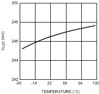 Figure 1. VCST vs Junction Temperature
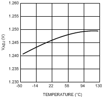 Figure 3. VADJ vs Junction Temperature
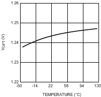 Figure 5. VOFT vs Junction Temperature
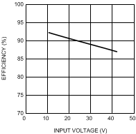 Figure 7. LM3409 Efficiency vs Input Voltage VO = 17 V (5 LEDs); ILED = 2 A
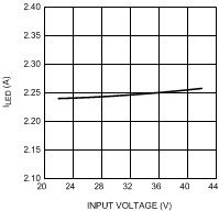 Figure 9. LM3409 LED Current vs Input Voltage VO = 17 V (5 LEDs)
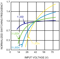 Figure 11. Normalized Switching Frequency vs Input Voltage
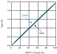 Figure 13. Internal EN Pin PWM Dimming VO = 17 V (5 LEDs); VIN = 24 V
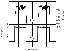
NOTE: The waveforms were acquired using the standard evaluation board from AN-1953 (SNVA390).
Figure 15. 20 kHz 50% EN Pin PWM Dimming VO = 42 V (12 LEDs); VIN = 48 V
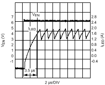
NOTE: The waveforms were acquired using the standard evaluation board from AN-1953 (SNVA390).
Figure 17. 20 kHz 50% EN Pin PWM Dimming (Rising Edge) VO = 42 V (12 LEDs); VIN = 48 V
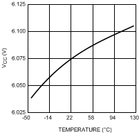 Figure 2. VCC vs Junction Temperature
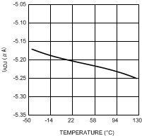 Figure 4. IADJ vs Junction Temperature
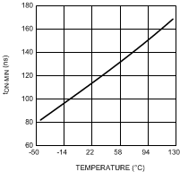 Figure 6. tON-MIN vs Junction Temperature
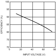 Figure 8. LM3409HV Efficiency vs Input Voltage VO = 17 V (5 LEDs); ILED = 2 A
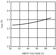 Figure 10. LM3409HV LED Current vs Input Voltage VO = 17 V (5 LEDs)
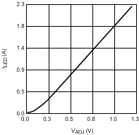 Figure 12. Amplitude Dimming Using IADJ Pin VO = 17 V (5 LEDs); VIN = 24 V
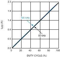 Figure 14. External Parallel FET PWM Dimming VO = 17 V (5 LEDs); VIN = 24 V
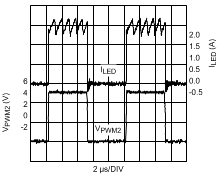
NOTE: The waveforms were acquired using the standard evaluation board from AN-1953 (SNVA390).
Figure 16. 100 kHz 50% External FET PWM Dimming VO = 42 V (12 LEDs); VIN = 48 V
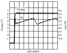
The waveforms were acquired using the standard evaluation board from AN-1953 (SNVA390).
Figure 18. 100 kHz 50% External FET PWM Dimming (Rising Edge) VO = 42 V (12 LEDs); VIN = 48 V