SNVS113F December 1999 – May 2016 LM3411
PRODUCTION DATA.
- 1 Features
- 2 Applications
- 3 Description
- 4 Revision History
- 5 Pin Configuration and Functions
- 6 Specifications
- 7 Parameter Measurement Information
- 8 Detailed Description
-
9 Application and Implementation
- 9.1 Application Information
- 9.2
Typical Applications
- 9.2.1 LM3411 Typical Application
- 9.2.2 Isolated 250-mA Flyback Switching Regulator
- 9.2.3 Isolated 1.5-A Flyback Switching Regulator
- 9.2.4 Precision 1-A Buck Regulator
- 9.2.5 Negative Input, Negative or Positive Output Flyback Regulator
- 9.2.6 Precision 5-V, 1-A Low Dropout Regulator
- 9.2.7 3.3-V, 0.5-A Low Dropout Regulator
- 9.2.8 Precision Positive Voltage Regulator With Accurate Current Limit
- 9.2.9 Precision Negative Voltage Regulator
- 9.2.10 4.7-V Power ON Detector With Hysteresis
- 9.2.11 ±50-mV External Trim
- 9.2.12 250-mA Shunt Regulator
- 9.2.13 Voltage Detector
- 9.2.14 Overvoltage Crowbar
- 10Power Supply Recommendations
- 11Layout
- 12Device and Documentation Support
- 13Mechanical, Packaging, and Orderable Information
Package Options
Mechanical Data (Package|Pins)
- DBV|5
Thermal pad, mechanical data (Package|Pins)
Orderable Information
1 Features
2 Applications
- Secondary Controller for Isolated DC-DC PWM Switching Regulators Systems
- Use With LDO Regulator for High-Precision, Fixed-Output Regulators
- Precision Monitoring Applications
- Use With Many Types of Regulators to Increase Precision and Improve Performance
3 Description
The LM3411 is a low-power fixed-voltage (3.3 V or
5 V) precision shunt regulator designed specifically for driving an optoisolator to provide feedback isolation in a switching regulator.
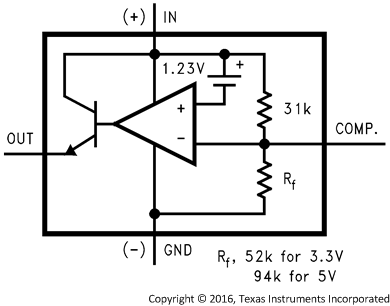
The LM3411 circuitry includes an internally compensated operational amplifier, a bandgap reference, NPN output transistor, and voltage setting resistors.
A trimmed precision bandgap reference with temperature drift curvature correction provides a ensured 1% precision over the operating temperature range (A grade version). The inverting input of the amplifier is externally accessible for loop frequency compensation when used as part of a larger servo system. The output is an open-emitter NPN transistor capable of driving up to 15 mA of load current.
Because of its small die size, the LM3411 has been made available in the subminiature 5-pin SOT-23 surface-mount package. This package is ideal for use in space-critical applications.
Although its main application is to provide a precision output voltage (no trimming required) and maintain very good regulation in isolated DC-DC converters, it can also be used with other types of voltage regulators or power semiconductors to provide a precision output voltage without precision resistors or trimming.
Device Information(1)
| PART NUMBER | PACKAGE | BODY SIZE (NOM) |
|---|---|---|
| LM3411 | SOT-23 (5) | 2.90 mm × 1.60 mm |
- For all available packages, see the orderable addendum at the end of the data sheet.
Typical Application Schematic

LM3411 Functional Diagram
