SNVS113F December 1999 – May 2016 LM3411
PRODUCTION DATA.
- 1 Features
- 2 Applications
- 3 Description
- 4 Revision History
- 5 Pin Configuration and Functions
- 6 Specifications
- 7 Parameter Measurement Information
- 8 Detailed Description
-
9 Application and Implementation
- 9.1 Application Information
- 9.2
Typical Applications
- 9.2.1 LM3411 Typical Application
- 9.2.2 Isolated 250-mA Flyback Switching Regulator
- 9.2.3 Isolated 1.5-A Flyback Switching Regulator
- 9.2.4 Precision 1-A Buck Regulator
- 9.2.5 Negative Input, Negative or Positive Output Flyback Regulator
- 9.2.6 Precision 5-V, 1-A Low Dropout Regulator
- 9.2.7 3.3-V, 0.5-A Low Dropout Regulator
- 9.2.8 Precision Positive Voltage Regulator With Accurate Current Limit
- 9.2.9 Precision Negative Voltage Regulator
- 9.2.10 4.7-V Power ON Detector With Hysteresis
- 9.2.11 ±50-mV External Trim
- 9.2.12 250-mA Shunt Regulator
- 9.2.13 Voltage Detector
- 9.2.14 Overvoltage Crowbar
- 10Power Supply Recommendations
- 11Layout
- 12Device and Documentation Support
- 13Mechanical, Packaging, and Orderable Information
Package Options
Mechanical Data (Package|Pins)
- DBV|5
Thermal pad, mechanical data (Package|Pins)
Orderable Information
8 Detailed Description
8.1 Overview
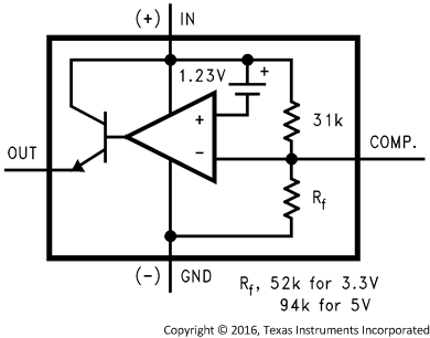
The LM3411 is a shunt regulator specifically designed to be the reference and control section in an overall feedback loop of a regulated power supply. The regulated output voltage is sensed between the IN pin and GROUND pin of the LM3411. If the voltage at the IN pin is less than the LM3411 regulating voltage (VREG), the OUT pin sources no current. As the voltage at the IN pin approaches the VREG voltage, the OUT pin begins sourcing current. This current is then used to drive a feedback device, (optocoupler) or a power device (linear regulator, switching regulator, and so forth) which serves the output voltage to be the same value as VREG.
In some applications (even under normal operating conditions), the voltage on the IN pin can be forced above the VREG voltage. In these instances, the maximum voltage applied to the IN pin should not exceed 20 V. In addition, an external resistor may be required on the OUT pin to limit the maximum current to 20 mA.
8.2 Functional Block Diagrams
 Figure 17. LM3411 Functional Diagram
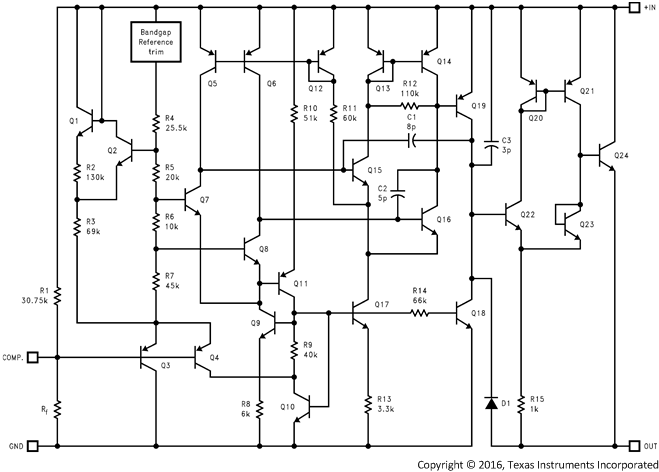
 Figure 18. Detailed Schematic
8.3 Feature Description
The LM3411 devices contain an internal operational amplifier, precision reference, feedback resister divider, and a bi-polar transistor suitable for driving an optocoupler. The divider resistor is sized such that the system will regulate the +IN pin to either 3.3 V or 5 V depending on the device version used. By connecting a feedback network from the OUT pin to the COMP pin, local compensation is implemented to stabilize the system.
8.4 Device Functional Modes
The primary mode of operation for the LM3411 is as a shunt regulator. In addition the device has robust overcurrent protection. These features make it applicable to a wide range of applications ranging from isolated feedback control to traditional shunt regulation.