SNVS570M January 2009 – November 2015 LM3445
PRODUCTION DATA.
- 1 Features
- 2 Applications
- 3 Description
- 4 Revision History
- 5 Pin Configuration and Functions
- 6 Specifications
-
7 Detailed Description
- 7.1 Overview
- 7.2 Functional Block Diagram
- 7.3
Feature Description
- 7.3.1 Overview of Phase Control Dimming
- 7.3.2 Theory of Operation
- 7.3.3 Sensing the Rectified TRIAC Waveform
- 7.3.4 LM3445 Line Sensing Circuitry
- 7.3.5 TRIAC Holding Current Resistor
- 7.3.6 Angle Detect
- 7.3.7 Bleeder
- 7.3.8 FLTR1 Pin
- 7.3.9 Dim Decoder
- 7.3.10 Valley-Fill Circuit
- 7.3.11 Valley-Fill Operation
- 7.3.12 Buck Converter
- 7.3.13 Overview of Constant Off-Time Control
- 7.3.14 Master/Slave Operation
- 7.3.15 Master/Slave Configuration
- 7.3.16 Master Board Modifications
- 7.3.17 Slave Board Modifications
- 7.3.18 Master/Slave Interconnection
- 7.3.19 Master/Slave Theory of Operation
- 7.3.20 Master/Slave Connection Diagram
- 7.3.21 Master/Slave Block Diagrams
- 7.3.22 Thermal Shutdown
- 7.4 Device Functional Modes
-
8 Application and Implementation
- 8.1 Application Information
- 8.2 Typical Application
- 9 Power Supply Recommendations
- 10Layout
- 11Device and Documentation Support
- 12Mechanical, Packaging, and Orderable Information
Package Options
Mechanical Data (Package|Pins)
Thermal pad, mechanical data (Package|Pins)
Orderable Information
8 Application and Implementation
NOTE
Information in the following applications sections is not part of the TI component specification, and TI does not warrant its accuracy or completeness. TI’s customers are responsible for determining suitability of components for their purposes. Customers should validate and test their design implementation to confirm system functionality.
8.1 Application Information
8.1.1 Determining Duty-Cycle (D)
As shown in Equation 4, duty cycle (D) approximately equals:

With efficiency considered:

For simplicity, choose efficiency between 75% and 85%.
8.1.2 Calculating Off-Time
The Off-Time of the LM3445 is set by the user and remains fairly constant as long as the voltage of the LED stack remains constant. Calculating the off-time is the first step in determining the switching frequency of the converter, which is integral in determining some external component values.
PNP transistor Q3, resistor R4, and the LED string voltage define a charging current into capacitor C11. A constant current into a capacitor creates a linear charging characteristic, as shown in Equation 6.

Resistor R4, capacitor C11 and the current through resistor R4 (iCOLL), which is approximately equal to VLED/R4, are all fixed. Therefore, dv is fixed and linear, and dt (tOFF) can now be calculated.

Equation 8 shows common equations for determining duty cycle and switching frequency in any buck converter.
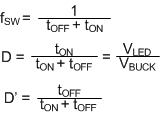
Therefore:

With efficiency of the buck converter in mind, as shown in Equation 10.

Substitute equations and rearrange:

Off-time, and switching frequency can now be calculated using the equations above.
8.1.3 Setting the Switching Frequency
Selecting the switching frequency for nominal operating conditions is based on tradeoffs between efficiency (better at low frequency) and solution size and cost (smaller at high frequency).
The input voltage to the buck converter (VBUCK) changes with both line variations and over the course of each half-cycle of the input line voltage. The voltage across the LED string will, however, remain constant, and therefore the off-time remains constant.
The on-time, and therefore the switching frequency, will vary as the VBUCK voltage changes with line voltage. A good design practice is to choose a desired nominal switching frequency knowing that the switching frequency will decrease as the line voltage drops and increase as the line voltage increases (see Figure 23).
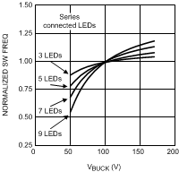 Figure 23. Graphical Illustration of Switching Frequency vs VBUCK
The off-time of the LM3445 can be programmed for switching frequencies ranging from 30 kHz to over 1 MHz. A trade-off between efficiency and solution size must be considered when designing the LM3445 application.
The maximum switching frequency attainable is limited only by the minimum on-time requirement (200 ns).
Worst case scenario for minimum on time is when VBUCK is at its maximum voltage (AC high line) and the LED string voltage (VLED) is at its minimum value.

The maximum voltage seen by the Buck Converter is:

8.1.4 Inductor Selection
The controlled off-time architecture of the LM3445 regulates the average current through the inductor (L2), and therefore the LED string current. The input voltage to the buck converter (VBUCK) changes with line variations and over the course of each half-cycle of the input line voltage. The voltage across the LED string is relatively constant, and therefore the current through R4 is constant. This current sets the off-time of the converter and therefore the output volt-second product (VLED x off-time) remains constant. A constant volt-second product makes it possible to keep the ripple through the inductor constant as the voltage at VBUCK varies.
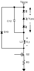 Figure 24. LM3445 External Components of the Buck Converter
The equation for an ideal inductor is shown in Equation 14.

Given a fixed inductor value, L, this equation states that the change in the inductor current over time is proportional to the voltage applied across the inductor.
During the on-time, the voltage applied across the inductor is,
Since the voltage across the MOSFET switch (Q2) is relatively small, as is the voltage across sense resistor R3, we can simplify this to approximately,
During the off-time, the voltage seen by the inductor is approximately:
The value of VL(OFF-TIME) will be relatively constant, because the LED stack voltage will remain constant. If we rewrite the equation for an inductor inserting what we know about the circuit during the off-time, we get Equation 18.

Re-arranging this gives us Equation 19.

From this we can see that the ripple current (Δi) is proportional to off-time (tOFF) multiplied by a voltage which is dominated by VLED divided by a constant (L2).
These equations can be rearranged to calculate the desired value for inductor L2.

Where:

Finally:

See Typical Application to better understand the design process.
8.1.5 Setting the LED Current
The LM3445 constant off-time control loop regulates the peak inductor current (IL2). The average inductor current equals the average LED current (IAVE). Therefore the average LED current is regulated by regulating the peak inductor current.
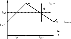 Figure 25. Inductor Current Waveform in CCM
Knowing the desired average LED current, IAVE and the nominal inductor current ripple, ΔiL, the peak current for an application running in continuous conduction mode (CCM) is defined in Equation 23.

Or, the maximum, or undimmed, LED current would then be,

This is important to calculate because this peak current multiplied by the sense resistor R3 will determine when the internal comparator is tripped. The internal comparator turns the control MOSFET off once the peak sensed voltage reaches 750 mV, as shown in Equation 25.

Current Limit: Under normal circumstances, the trip voltage on the PWM comparator would be less than or equal to 750 mV, depending on the amount of dimming. However, if there is a short circuit or an excessive load on the output, higher than normal switch currents will cause a voltage above 1.27 V on the ISNS pin which will trip the I-LIM comparator. The I-LIM comparator will reset the RS latch, turning off Q2. It will also inhibit the Start Pulse Generator and the COFF comparator by holding the COFF pin low. A delay circuit will prevent the start of another cycle for 180 µs.
8.1.6 Valley Fill Capacitors
Determining voltage rating and capacitance value of the valley-fill capacitors:
Equation 26 shows the maximum voltage seen by the valley-fill capacitors is:

This is, of course, if the capacitors chosen have identical capacitance values and split the line voltage equally. Often a 20% difference in capacitance could be observed between like capacitors. Therefore a voltage rating margin of 25% to 50% should be considered.
8.1.6.1 Determining the Capacitance Value of the Valley-Fill Capacitors
The valley fill capacitors should be sized to supply energy to the buck converter (VBUCK) when the input line is less than its peak divided by the number of stages used in the valley fill (tX). The capacitance value should be calculated when the TRIAC is not firing, that is, when full LED current is being drawn by the LED string. The maximum power is delivered to the LED string at this time, and therefore the most capacitance is required.
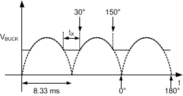 Figure 26. Two Stage Valley-Fill VBUCK Voltage With No TRIAC Dimming
From the above illustration and the equation for current in a capacitor, i = C × dV/dt, the amount of capacitance needed at VBUCK is calculated as follows:
At 60Hz, and a valley-fill circuit of two stages, the hold up time (tX) required at VBUCK is calculated as follows. The total angle of an AC half cycle is 180° and the total time of a half AC line cycle is 8.33 ms. When the angle of the AC waveform is at 30° and 150°, the voltage of the AC line is exactly ½ of its peak. With a two stage valley-fill circuit, this is the point where the LED string switches from power being derived from AC line to power being derived from the hold up capacitors (C7 and C9). 60° out of 180° of the cycle or 1/3 of the cycle the power is derived from the hold up capacitors (1/3 × 8.33 ms = 2.78 ms). This is equal to the hold up time (dt) from the above equation, and dv is the amount of voltage the circuit is allowed to droop. From the next section (“Determining Maximum Number of Series Connected LEDs Allowed”) we know the minimum VBUCK voltage will be about 45 V for a 90 VAC to 135 VAC line. At 90 VAC low line operating condition input, ½ of the peak voltage is 64 V. Therefore, with some margin the voltage at VBUCK can not droop more than about 15 V (dv). (i) is equal to (POUT/VBUCK), where POUT is equal to (VLED × ILED). Total capacitance (C7 in parallel with C9) can now be calculated. See Typical Application for further calculations of the valley-fill capacitors.
8.1.6.2 Determining Maximum Number of Series Connected LEDs Allowed
The LM3445 is an off-line buck topology LED driver. A buck converter topology requires that the input voltage (VBUCK) of the output circuit must be greater than the voltage of the LED stack (VLED) for proper regulation. One must determine what the minimum voltage observed by the buck converter will be before the maximum number of LEDs allowed can be determined. Two variables will have to be determined in order to accomplish this.
- AC line operating voltage. This is usually 90 VAC to 135 VAC for North America. Although the LM3445 can operate at much lower and higher input voltages a range is needed to illustrate the design process.
- How many stages are implemented in the valley-fill circuit (1, 2 or 3).
In this example the most common valley-fill circuit will be used (two stages).
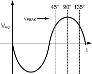 Figure 27. AC Line with Firing Angles
Figure 28 shows three TRIAC dimmed waveforms. One can easily see that the peak voltage (VPEAK) from 0° to 90° will always be:

Once the TRIAC is firing at an angle greater than 90° the peak voltage will lower and equal to Equation 28.

The voltage at VBUCK with a valley fill stage of two will look similar to the waveforms of Figure 29.
The purpose of the valley fill circuit is to allow the buck converter to pull power directly off of the AC line when the line voltage is greater than its peak voltage divided by two (two stage valley fill circuit). During this time, the capacitors within the valley fill circuit (C7 and C8) are charged up to the peak of the AC line voltage. Once the line drops below its peak divided by two, the two capacitors are placed in parallel and deliver power to the buck converter. One can now see that if the peak of the AC line voltage is lowered due to variations in the line voltage, or if the TRIAC is firing at an angle above 90°, the DC offset (VDC) will lower. VDC is the lowest value that voltage VBUCK will encounter.

Example:
Line voltage = 90 VAC to 135 VAC
Valley-Fill = two stage

Depending on what type and value of capacitors are used, some derating should be used for voltage droop when the capacitors are delivering power to the buck converter. When the TRIAC is firing at 135° the current through the LED string will be small. Therefore the droop should be small at this point and a 5% voltage droop should be a sufficient derating. With this derating, the lowest voltage the buck converter will see is about 42.5 V in this example.
 Figure 28. AC Line With Various Firing Angles
 Figure 29. VBUCK Waveforms With Various Firing Angles
To determine how many LEDs can be driven, take the minimum voltage the buck converter will see (42.5 V) and divide it by the worst case forward voltage drop of a single LED.
Example: 42.5 V / 3.7 V = 11.5 LEDs (11 LEDs with margin)
8.1.7 Output Capacitor
A capacitor placed in parallel with the LED or array of LEDs can be used to reduce the LED current ripple while keeping the same average current through both the inductor and the LED array. With a buck topology the output inductance (L2) can now be lowered, making the magnetics smaller and less expensive. With a well designed converter, you can assume that all of the ripple will be seen by the capacitor, and not the LEDs. One must ensure that the capacitor you choose can handle the RMS current of the inductor. See manufacture’s data sheets to ensure compliance. Usually an X5R or X7R capacitor between 1 µF and 10 µF of the proper voltage rating will be sufficient.
8.1.8 Switching MOSFET
The main switching MOSFET should be chosen with efficiency and robustness in mind. The maximum voltage across the switching MOSFET will equal:

The average current rating should be greater than:
8.1.9 Re-Circulating Diode
The LM3445 Buck converter requires a re-circulating diode D10 (see the Typical Application circuit to carry the inductor current during the MOSFET Q2 off-time. The most efficient choice for D10 is a diode with a low forward drop and near-zero reverse recovery time that can withstand a reverse voltage of the maximum voltage seen at VBUCK. For a common 110 VAC ± 20% line, the reverse voltage could be as high as 190 V.

The current rating must be at least:
Or:

8.2 Typical Application
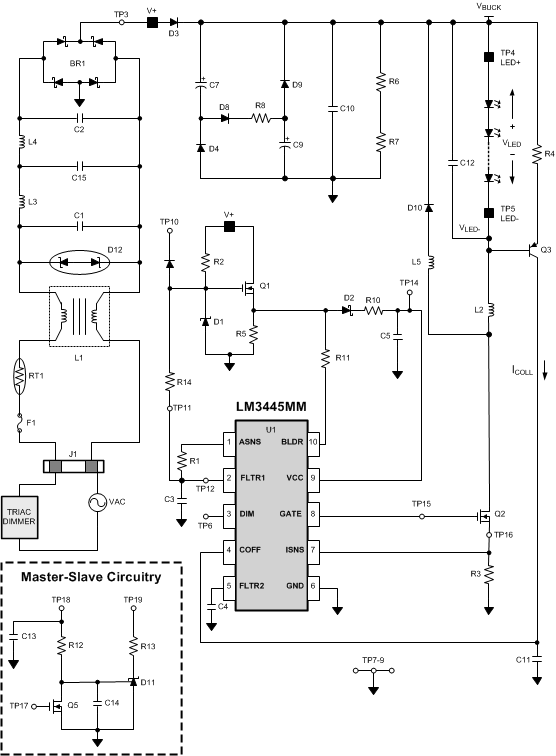 Figure 30. LM3445 Design Example 1 Input = 90 VAC to 135 VAC, VLED = 7 × HB LED String Application at 400 MA
8.2.1 Design Requirements
Known:
- Input voltage range (90 VAC – 135 VAC)
- Number of LEDs in series = 7
- Forward voltage drop of a single LED = 3.6 V
- LED stack voltage = (7 × 3.6V) = 25.2 V
Choose:
- Nominal switching frequency, fSW-TARGET = 350 kHz
- ILED(AVE) = 400 mA
- Δi (usually 15% - 30% of ILED(AVE)) = (0.30 × 400 mA) = 120 mA
- Valley fill stages (1, 2, or 3) = 2
- Assumed minimum efficiency = 80%
8.2.2 Detailed Design Procedure
The following design example illustrates the process of calculating external component values.
Calculate:
- Calculate minimum voltage VBUCK equals:
- Calculate maximum voltage VBUCK equals:
- Calculate tOFF at VBUCK nominal line voltage:
- Calculate tON(MIN) at high line to ensure that tON(MIN) > 200 ns:
- Calculate C11 and R4:
- Choose current through R4: (between 50 µA and 100 µA) 70 µA
- Use a standard value of 365 kΩ
- Calculate C11:
- Use standard value of 120 pF
- Calculate ripple current: 400 mA × 0.30 = 120 mA
- Calculate inductor value at tOFF = 3 µs:
- Choose C10: 1 µF 200 V
- Calculate valley-fill capacitor values: VAC low line = 90 VAC, VBUCK minimum equals 60 V (no TRIAC dimming at maximum LED current). Set droop for 20 V maximum at full load and low line.
- i equals POUT / VBUCK (270 mA).
- dV equals 20 V.
- dt equals 2.77 ms.
- CTOTAL equals 37 µF.


where
Table 1. Bill of Materials
8.2.3 Application Curve
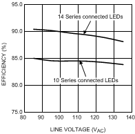 Figure 31. Efficiency versus Input Voltage