SNVS570M January 2009 – November 2015 LM3445
PRODUCTION DATA.
- 1 Features
- 2 Applications
- 3 Description
- 4 Revision History
- 5 Pin Configuration and Functions
- 6 Specifications
-
7 Detailed Description
- 7.1 Overview
- 7.2 Functional Block Diagram
- 7.3
Feature Description
- 7.3.1 Overview of Phase Control Dimming
- 7.3.2 Theory of Operation
- 7.3.3 Sensing the Rectified TRIAC Waveform
- 7.3.4 LM3445 Line Sensing Circuitry
- 7.3.5 TRIAC Holding Current Resistor
- 7.3.6 Angle Detect
- 7.3.7 Bleeder
- 7.3.8 FLTR1 Pin
- 7.3.9 Dim Decoder
- 7.3.10 Valley-Fill Circuit
- 7.3.11 Valley-Fill Operation
- 7.3.12 Buck Converter
- 7.3.13 Overview of Constant Off-Time Control
- 7.3.14 Master/Slave Operation
- 7.3.15 Master/Slave Configuration
- 7.3.16 Master Board Modifications
- 7.3.17 Slave Board Modifications
- 7.3.18 Master/Slave Interconnection
- 7.3.19 Master/Slave Theory of Operation
- 7.3.20 Master/Slave Connection Diagram
- 7.3.21 Master/Slave Block Diagrams
- 7.3.22 Thermal Shutdown
- 7.4 Device Functional Modes
-
8 Application and Implementation
- 8.1 Application Information
- 8.2 Typical Application
- 9 Power Supply Recommendations
- 10Layout
- 11Device and Documentation Support
- 12Mechanical, Packaging, and Orderable Information
Package Options
Mechanical Data (Package|Pins)
Thermal pad, mechanical data (Package|Pins)
Orderable Information
6 Specifications
6.1 Absolute Maximum Ratings
See(1) (3)(2)| MIN | MAX | UNIT | |
|---|---|---|---|
| BLDR to GND | –0.3 | 17 | V |
| VCC, GATE, FLTR1 to GND | –0.3 | 14 | V |
| ISNS to GND | –0.3 | 2.5 | V |
| ASNS, DIM, FLTR2, COFF to GND | –0.3 | 7 | V |
| COFF Input Current | 100 | mA | |
| Continuous Power Dissipation(4) | Internally Limited | ||
| Junction Temperature (TJ-MAX) | 150 | °C | |
| Storage Temperature | –65 | 150 | °C |
(1) Stresses beyond those listed under Absolute Maximum Ratings may cause permanent damage to the device. These are stress ratings only, which do not imply functional operation of the device at these or any other conditions beyond those indicated under Recommended Operating Conditions. Exposure to absolute-maximum-rated conditions for extended periods may affect device reliability
(2) All voltages are with respect to the potential at the GND pin, unless otherwise specified.
(3) If Military/Aerospace specified devices are required, please contact the Texas Instruments Sales Office/Distributors for availability and specifications.
(4) Internal thermal shutdown circuitry protects the device from permanent damage. Thermal shutdown engages at TJ = 165°C (typ.) and disengages at +TJ = 145°C (typ).
6.2 ESD Ratings
| VALUE | UNIT | |||
|---|---|---|---|---|
| V(ESD) | Electrostatic discharge | Human-body model (HBM), per ANSI/ESDA/JEDEC JS-001(1)(3) | ±2000 | V |
| Charged-device model (CDM), per JEDEC specification JESD22-C101(2) | ±1000 | |||
(1) JEDEC document JEP155 states that 500-V HBM allows safe manufacturing with a standard ESD control process.
(2) JEDEC document JEP157 states that 250-V CDM allows safe manufacturing with a standard ESD control process.
(3) Human Body Model, applicable std. JESD22-A114-C.
6.3 Recommended Operating Conditions
| MIN | MAX | UNIT | |
|---|---|---|---|
| VCC | 8 | 12 | V |
| Junction Temperature | –40 | 125 | °C |
6.4 Thermal Information
| THERMAL METRIC(1) | LM3445 | UNIT | ||
|---|---|---|---|---|
| DGS (VSSOP) | D (SOIC) | |||
| 10 PINS | 14 PINS | |||
| RθJA | Junction-to-ambient thermal resistance | 159 | 82.8 | °C/W |
| RθJC(top) | Junction-to-case (top) thermal resistance | 54.5 | 40.2 | °C/W |
| RθJB | Junction-to-board thermal resistance | 78.7 | 37.5 | °C/W |
| ψJT | Junction-to-top characterization parameter | 5.3 | 6.4 | °C/W |
| ψJB | Junction-to-board characterization parameter | 77.5 | 37.2 | °C/W |
| RθJC(bot) | Junction-to-case (bottom) thermal resistance | N/A | N/A | °C/W |
(1) For more information about traditional and new thermal metrics, see the Semiconductor and IC Package Thermal Metrics application report, SPRA953.
6.5 Electrical Characteristics
All Typical limits are for TJ = 25°C and all Maximum and Minimum limits apply over the full Operating Temperature Range ( TJ = −40°C to +125°C). Minimum and Maximum limits are specified through test, design, or statistical correlation. Typical values represent the most likely parametric norm at TJ = +25ºC, and are provided for reference purposes only.| PARAMETER | TEST CONDITIONS | MIN | TYP | MAX | UNIT | |
|---|---|---|---|---|---|---|
| BLEEDER | ||||||
| RBLDR | Bleeder resistance to GND | IBLDR = 10 mA | 230 | 325 | Ω | |
| VCC SUPPLY | ||||||
| IVCC | Operating supply current | 2 | 2.85 | mA | ||
| VCC-UVLO | Rising threshold | 7.4 | 7.7 | V | ||
| Falling threshold | 6 | 6.4 | ||||
| Hysterisis | 1 | |||||
| COFF | ||||||
| VCOFF | Time out threshold | 1.225 | 1.276 | 1.327 | V | |
| RCOFF | Off timer sinking impedance | 33 | 60 | Ω | ||
| tCOFF | Restart timer | 180 | µs | |||
| CURRENT LIMIT | ||||||
| VISNS | ISNS limit threshold | 1.174 | 1.269 | 1.364 | V | |
| tISNS | Leading edge blanking time | 125 | ns | |||
| Current limit reset delay | 180 | µs | ||||
| ISNS limit to GATE delay | ISNS = 0 to 1.75-V step | 33 | ns | |||
| INTERNAL PWM RAMP | ||||||
| fRAMP | Frequency | 5.85 | kHz | |||
| VRAMP | Valley voltage | 0.96 | 1 | 1.04 | V | |
| Peak voltage | 2.85 | 3 | 3.08 | |||
| DRAMP | Maximum duty cycle | 96.5% | 98% | |||
| DIM DECODER | ||||||
| tANG_DET | Angle detect rising threshold | Observed on BLDR pin | 6.79 | 7.21 | 7.81 | V |
| VASNS | ASNS filter delay | 4 | µs | |||
| ASNS VMAX | 3.85 | 4 | 4.15 | V | ||
| IASNS | ASNS drive capability sink | VASNS = 2 V | 7.6 | mA | ||
| ASNS drive capability source | VASNS = 2 V | –4.3 | ||||
| DIM low sink current | VDIM = 1 V | 1.65 | 2.8 | |||
| DIM High source current | VDIM = 4 V | –4 | –3 | |||
| VDIM | DIM low voltage | PWM input voltage threshold | 0.9 | 1.33 | V | |
| DIM high voltage | 2.33 | 3.15 | ||||
| VTSTH | Tri-state threshold voltage | Apply to FLTR1 pin | 4.87 | 5.25 | V | |
| RDIM | DIM comparator tri-state impedance | 10 | MΩ | |||
| CURRENT SENSE COMPARATOR | ||||||
| VFLTR2 | FLTR2 open circuit voltage | 720 | 750 | 780 | mV | |
| RFLTR2 | FLTR2 impedance | 420 | kΩ | |||
| VOS | Current sense comparator offset voltage | –4 | 0.1 | 4 | mV | |
| GATE DRIVE OUTPUT | ||||||
| VDRVH | GATE high saturation | IGATE = 50 mA | 0.24 | 0.5 | V | |
| VDRVL | GATE low saturation | IGATE = 100 mA | 0.22 | 0.5 | ||
| IDRV | Peak souce current | GATE = VCC/2 | –0.77 | A | ||
| Peak sink current | GATE = VCC/2 | 0.88 | ||||
| tDV | Rise time | Cload = 1 nF | 15 | ns | ||
| Fall time | Cload = 1 nF | 15 | ||||
| THERMAL SHUTDOWN | ||||||
| TSD | Thermal shutdown temperature | See (1) | 165 | °C | ||
| Thermal shutdown hysteresis | 20 | |||||
(1) Junction-to-ambient thermal resistance is highly application and board-layout dependent. In applications where high maximum power dissipation exists, special care must be paid to thermal dissipation issues in board design. In applications where high power dissipation and/or poor package thermal resistance is present, the maximum ambient temperature may have to be derated. Maximum ambient temperature (TA-MAX) is dependent on the maximum operating junction temperature (TJ-MAX-OP = 125°C), the maximum power dissipation of the device in the application (PD-MAX), and the junction-to ambient thermal resistance of the part/package in the application (RθJA), as given by the following equation: TA-MAX = TJ-MAX-OP – (RθJA × PD-MAX).
6.6 Typical Characteristics
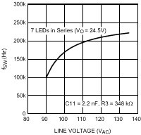 Figure 1. fSW vs Input Line Voltage
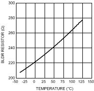 Figure 3. BLDR Resistor vs Temperature
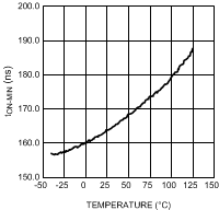 Figure 5. Min On-Time (tON) vs Temperature
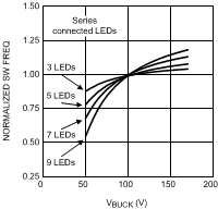 Figure 7. Normalized Variation in fSW over VBUCK Voltage
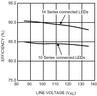 Figure 2. Efficiency vs Input Line Voltage
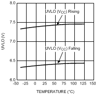 Figure 4. VCC UVLO vs Temperature
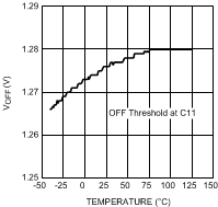 Figure 6. Off Threshold (C11) vs Temperature
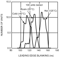 Figure 8. Leading Edge Blanking Variation Over Temperature