SNIS159H August 1999 – December 2017 LM35
PRODUCTION DATA.
- 1 Features
- 2 Applications
- 3 Description
- 4 Revision History
- 5 Pin Configuration and Functions
-
6 Specifications
- 6.1 Absolute Maximum Ratings
- 6.2 ESD Ratings
- 6.3 Recommended Operating Conditions
- 6.4 Thermal Information
- 6.5 Electrical Characteristics: LM35A, LM35CA Limits
- 6.6 Electrical Characteristics: LM35A, LM35CA
- 6.7 Electrical Characteristics: LM35, LM35C, LM35D Limits
- 6.8 Electrical Characteristics: LM35, LM35C, LM35D
- 6.9 Typical Characteristics
- 7 Detailed Description
- 8 Application and Implementation
- 9 Power Supply Recommendations
- 10Layout
- 11Device and Documentation Support
- 12Mechanical, Packaging, and Orderable Information
Package Options
Refer to the PDF data sheet for device specific package drawings
Mechanical Data (Package|Pins)
- D|8
- NDV|3
- LP|3
- NEB|3
Thermal pad, mechanical data (Package|Pins)
Orderable Information
7 Detailed Description
7.1 Overview
The LM35-series devices are precision integrated-circuit temperature sensors, with an output voltage linearly proportional to the Centigrade temperature. The LM35 device has an advantage over linear temperature sensors calibrated in Kelvin, as the user is not required to subtract a large constant voltage from the output to obtain convenient Centigrade scaling. The LM35 device does not require any external calibration or trimming to provide typical accuracies of ± ¼ °C at room temperature and ± ¾ °C over a full −55°C to 150°C temperature range. Lower cost is assured by trimming and calibration at the wafer level. The low output impedance, linear output, and precise inherent calibration of the LM35 device makes interfacing to readout or control circuitry especially easy. The device is used with single power supplies, or with plus and minus supplies. As the LM35 device draws only 60 μA from the supply, it has very low self-heating of less than 0.1°C in still air. The LM35 device is rated to operate over a −55°C to 150°C temperature range, while the LM35C device is rated for a −40°C to 110°C range (−10° with improved accuracy). The temperature-sensing element is comprised of a delta-V BE architecture.
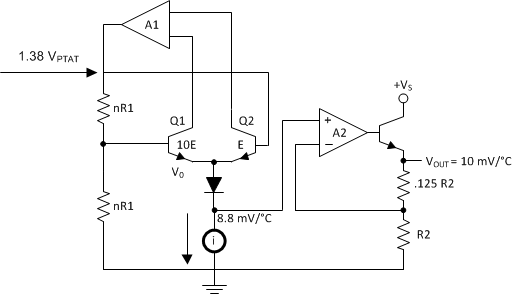
The temperature-sensing element is then buffered by an amplifier and provided to the VOUT pin. The amplifier has a simple class A output stage with typical 0.5-Ω output impedance as shown in the Functional Block Diagram. Therefore the LM35 can only source current and it's sinking capability is limited to 1 μA.
7.2 Functional Block Diagram

7.3 Feature Description
7.4 Device Functional Modes
The only functional mode of the LM35 is that it has an analog output directly proportional to temperature.