SNVS606L June 2009 – December 2014 LM3530
PRODUCTION DATA.
- 1 Features
- 2 Applications
- 3 Description
- 4 Revision History
- 5 I2C Device Options
- 6 Pin Configuration and Functions
- 7 Specifications
-
8 Detailed Description
- 8.1 Overview
- 8.2 Functional Block Diagram
- 8.3
Feature Description
- 8.3.1 Start-Up
- 8.3.2 Light Load Operation
- 8.3.3 Ambient Light Sensor
- 8.3.4 ALS Operation
- 8.3.5 ALS Averaging Time
- 8.3.6 Zone Boundary Settings
- 8.3.7 Zone Boundary Trip Points and Hysteresis
- 8.3.8 Minimum Zone Boundary Settings
- 8.3.9 LED Current Control
- 8.3.10 Exponential or Linear Brightness Mapping Modes
- 8.3.11 PWM Input Polarity
- 8.3.12 I2C-Compatible Current Control Only
- 8.3.13 Simple Enable Disable With PWM Current Control
- 8.3.14 Ambient Light Current Control
- 8.3.15 Ambient Light Current Control + PWM
- 8.3.16 Interrupt Output
- 8.3.17 Overvoltage Protection
- 8.3.18 Hardware Enable
- 8.3.19 Thermal Shutdown
- 8.4 Device Functional Modes
- 8.5 Programming
- 8.6 Register Maps
- 9 Application and Implementation
- 10Power Supply Recommendations
- 11Layout
- 12Device and Documentation Support
- 13Mechanical, Packaging, and Orderable Information
Package Options
Mechanical Data (Package|Pins)
Thermal pad, mechanical data (Package|Pins)
Orderable Information
9 Application and Implementation
NOTE
Information in the following applications sections is not part of the TI component specification, and TI does not warrant its accuracy or completeness. TI’s customers are responsible for determining suitability of components for their purposes. Customers should validate and test their design implementation to confirm system functionality.
9.1 Application Information
The LM3530 incorporates a 40-V (maximum output) boost, a single current sink, and a dual ambient light sensor interface. The maximum boost output voltage is 40 V (min) for the LM3530-40 version. The LM3530 boost will drive the output voltage to whatever voltage necessary to maintain 400mV at the ILED input. The 40-V max output typically allows the LM3530 to drive from 2 series up to 12 series LEDs (3.2V max voltage per LED). For applications that do not use one or both of the ALS inputs, the ALS input can be connected to GND or left floating.
9.2 Typical Application
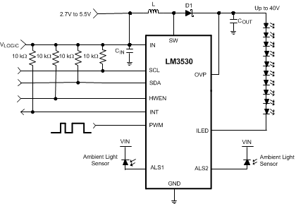 Figure 49. LM3530 Typical Application
9.2.1 Design Requirements
Example requirements for typical voltage inverter applications:
Table 12. Design Parameters
| DESIGN PARAMETER | EXAMPLE VALUE |
|---|---|
| Input voltage range | 2.7 V to 5.5 V |
| Output current | 0 mA to 30 mA |
| Boost switching frequency | 500 kHz |
Table 13. Application Circuit Component List
| COMPONENT | MANUFACTURER | PART NUMBER | VALUE | SIZE | CURRENT/VOLTAGE RATING |
|---|---|---|---|---|---|
| L | TDK | VLF3014ST100MR82 | 10 µH | 3 mm × 3 mm × 1.4 mm | ISAT = 820 mA |
| COUT | Murata | GRM21BR71H105KA12 | 1 µF | 0805 | 50 V |
| CIN | Murata | GRM188B31A225KE33 | 2.2 µF | 0603 | 10 V |
| D1 | Diodes Inc. | B0540WS | Schottky | SOD-323 | 40 V/500 mA |
| ALS1 | Avago | APDS-9005 | Ambient Light Sensor | 1.6 mm x 1.5 mm × 0.6 mm | 0 to 1100 Lux |
| ALS2 | Avago | APDS-9005 | Ambient Light Sensor | 1.6 mm x 1.5 mm × 0.6 mm | 0 to 1100 Lux |
9.2.2 Detailed Design Procedure
9.2.2.1 LED Current Setting/Maximum LED Current
The maximum LED current is restricted by the following factors: the maximum duty cycle that the boost converter can achieve, the peak current limitations, and the maximum output voltage.
9.2.2.2 Maximum Duty Cycle
The LM3530 can achieve up to typically 94% maximum duty cycle. Two factors can cause the duty cycle to increase: an increase in the difference between VOUT and VIN and a decrease in efficiency. This is shown by Equation 12:

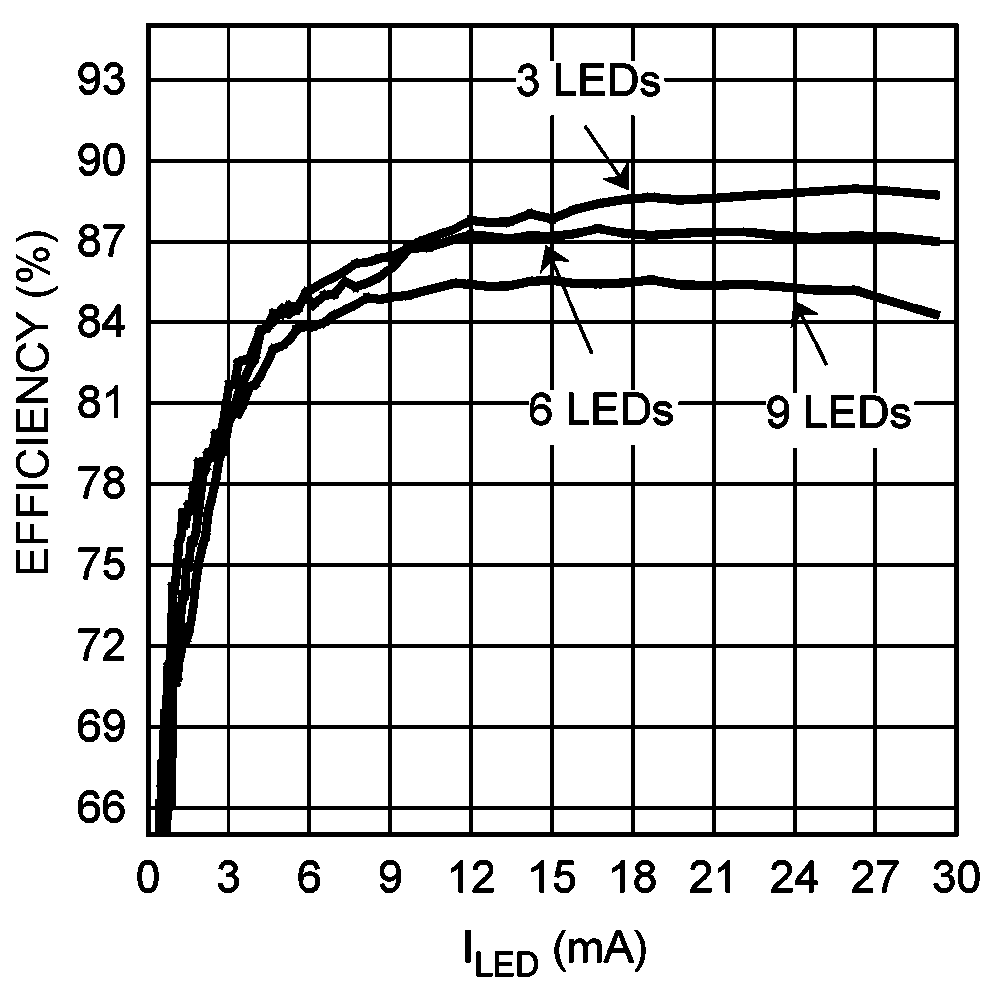
For a 9-LED configuration VOUT = (3.6 V x 9LED + VHR) = 33 V operating with η = 70% from a 3-V battery, the duty cycle requirement would be around 93.6%. Lower efficiency or larger VOUT to VIN differentials can push the duty cycle requirement beyond 94%.
9.2.2.3 Peak Current Limit
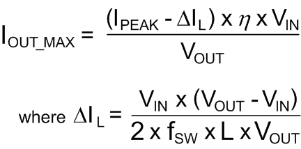
The LM3530 boost converter has a peak current limit for the internal power switch of 839 mA typical (739 mA minimum). When the peak switch current reaches the current limit, the duty cycle is terminated resulting in a limit on the maximum output current and thus the maximum output power the LM3530 can deliver. Calculate the maximum LED current as a function of VIN, VOUT, L, efficiency (η) and IPEAK as:
where
- ƒSW = 500 kHz
- η and IPEAK can be found in the Efficiency and IPEAK curves in the Specifications and Application Curves.
9.2.2.4 Output Voltage Limitations
The LM3530 has a maximum output voltage of 41 V typical (40 V minimum) for the LM3530-40 version and 24 V typical (23.6 V minimum) for the LM3530-25 version. When the output voltage rises above this threshold (VOVP) the overvoltage protection feature is activated and the duty cycle is terminated. Switching will cease until VOUT drops below the hysteresis level (typically 1 V below VOVP). For larger numbers of series connected LEDs the output voltage can reach the OVP threshold at larger LED currents and colder ambient temperatures. Typically white LEDs have a –3mV/°C temperature coefficient.
9.2.2.5 Output Capacitor Selection
The LM3530’s output capacitor has two functions: filtering of the boost converters switching ripple, and to ensure feedback loop stability. As a filter, the output capacitor supplies the LED current during the boost converters on time and absorbs inductor energy during the switch off time. This causes a sag in the output voltage during the on time and a rise in the output voltage during the off time. Because of this, the output capacitor must be sized large enough to filter the inductor current ripple that could cause the output voltage ripple to become excessive. As a feedback loop component, the output capacitor must be at least 1 µF and have low ESR otherwise the LM3530 boost converter can become unstable. This requires the use of ceramic output capacitors. Table 14 lists part numbers and voltage ratings for different output capacitors that can be used with the LM3530.
Table 14. Recommended Input/Output Capacitors
| MANUFACTURER | PART NUMBER | VALUE (µF) | SIZE | RATING (V) | DESCRIPTION |
|---|---|---|---|---|---|
| Murata | GRM21BR71H105KA12 | 1 | 0805 | 50 | COUT |
| Murata | GRM188B31A225KE33 | 2.2 | 0805 | 10 | CIN |
| TDK | C1608X5R0J225 | 2.2 | 0603 | 6.3 | CIN |
9.2.2.6 Inductor Selection
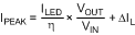
The LM3530 is designed to work with a 10-µH to 22-µH inductor. When selecting the inductor, ensure that the saturation rating for the inductor is high enough to accommodate the peak inductor current. Equation 14 and Equation 15 calculate the peak inductor current based upon LED current, VIN, VOUT, and efficiency.
where:
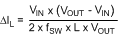
When choosing L, the inductance value must also be large enough so that the peak inductor current is kept below the LM3530 switch current limit. This forces a lower limit on L given by Equation 16.
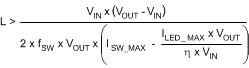
ISW_MAX is given in , efficiency (η) is shown in the Application Curves, and ƒSW is typically 500 kHz.
Table 15. Suggested Inductors
| MANUFACTURER | PART NUMBER | VALUE (µH) | SIZE (mm) | RATING (mA) | DC RESISTANCE (Ω) |
|---|---|---|---|---|---|
| TDK | VLF3014ST-100MR82 | 10 | 2.8 × 3 × 1.4 | 820 | 0.25 |
| TDK | VLF3010ST-220MR34 | 22 | 2.8 × 3 × 1 | 340 | 0.81 |
| TDK | VLF3010ST-100MR53 | 10 | 2.8 × 3 × 1 | 530 | 0.41 |
| TDK | VLF4010ST-100MR80 | 10 | 2.8 × 3 × 1 | 800 | 0.25 |
| TDK | VLS252010T-100M | 10 | 2.5 × 2 × 1 | 650 | 0.71 |
| Coilcraft | LPS3008-103ML | 10 | 2.95 × 2.95 × 0.8 | 520 | 0.65 |
| Coilcraft | LPS3008-223ML | 22 | 2.95 × 2.95 × 0.8 | 340 | 1.5 |
| Coilcraft | LPS3010-103ML | 10 | 2.95 × 2.95 × 0.9 | 550 | 0.54 |
| Coilcraft | LPS3010-223ML | 22 | 2.95 × 2.95 × 0.9 | 360 | 1.2 |
| Coilcraft | XPL2010-103ML | 10 | 1.9 × 2 × 1 | 610 | 0.56 |
| Coilcraft | EPL2010-103ML | 10 | 2 × 2 × 1 | 470 | 0.91 |
| TOKO | DE2810C-1117AS-100M | 10 | 3 × 3.2 × 1 | 600 | 0.46 |
9.2.2.7 Diode Selection
The diode connected between SW and OUT must be a Schottky diode and have a reverse breakdown voltage high enough to handle the maximum output voltage in the application. Table 16 lists various diodes that can be used with the LM3530. For 25-V OVP devices a 30-V Schottky is adequate. For 40-V OVP devices, a 40-V Schottky diode should be used.
Table 16. Suggested Diodes
| MANUFACTURER | PART NUMBER | VALUE | SIZE (mm) | RATING |
|---|---|---|---|---|
| Diodes Inc | B0540WS | Schottky | SOD-323 (1.7 × 1.3) | 40 V/500 mA |
| Diodes Inc | SDM20U40 | Schottky | SOD-523 (1.2 × 0.8 × 0.6) | 40 V/200 mA |
| On Semiconductor | NSR0340V2T1G | Schottky | SOD-523 (1.2 × 0.8 × 0.6) | 40 V/250 mA |
| On Semiconductor | NSR0240V2T1G | Schottky | SOD-523 (1.2 × 0.8 × 0.6) | 40 V/250 mA |
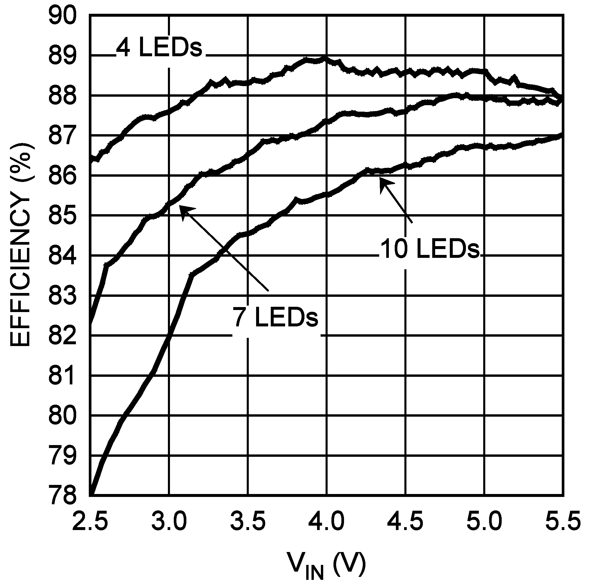
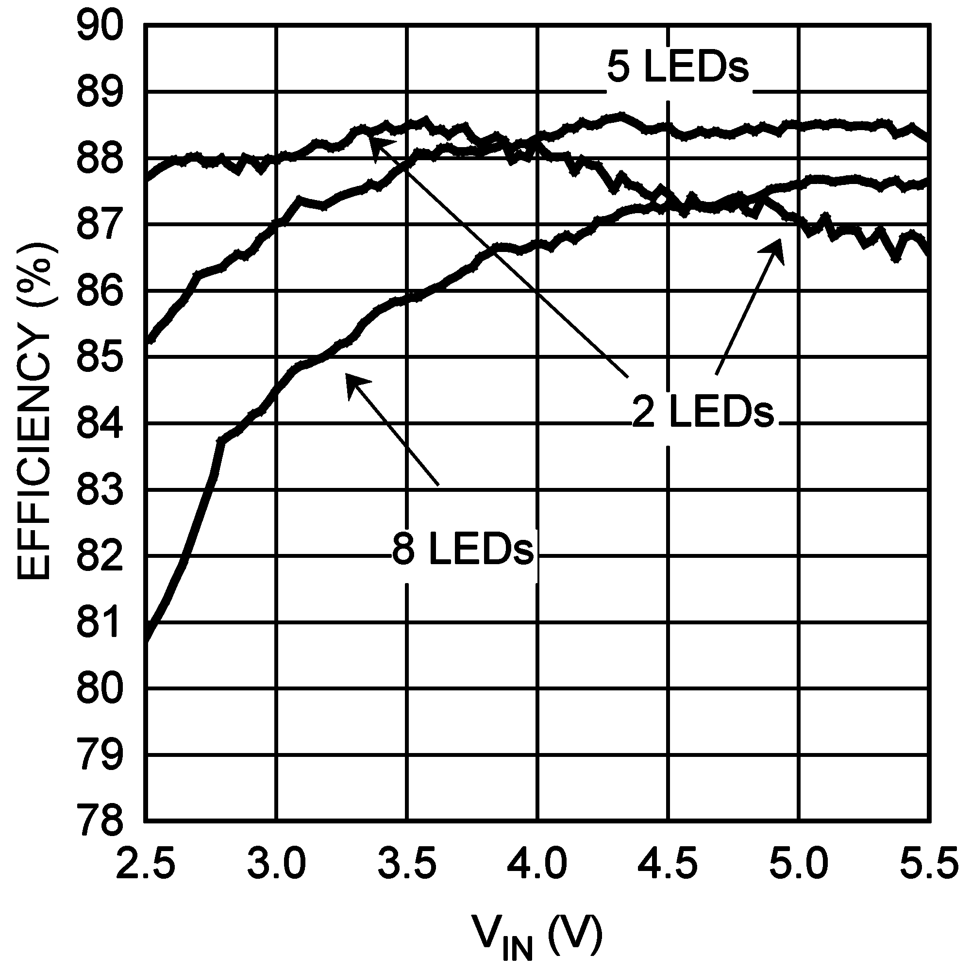
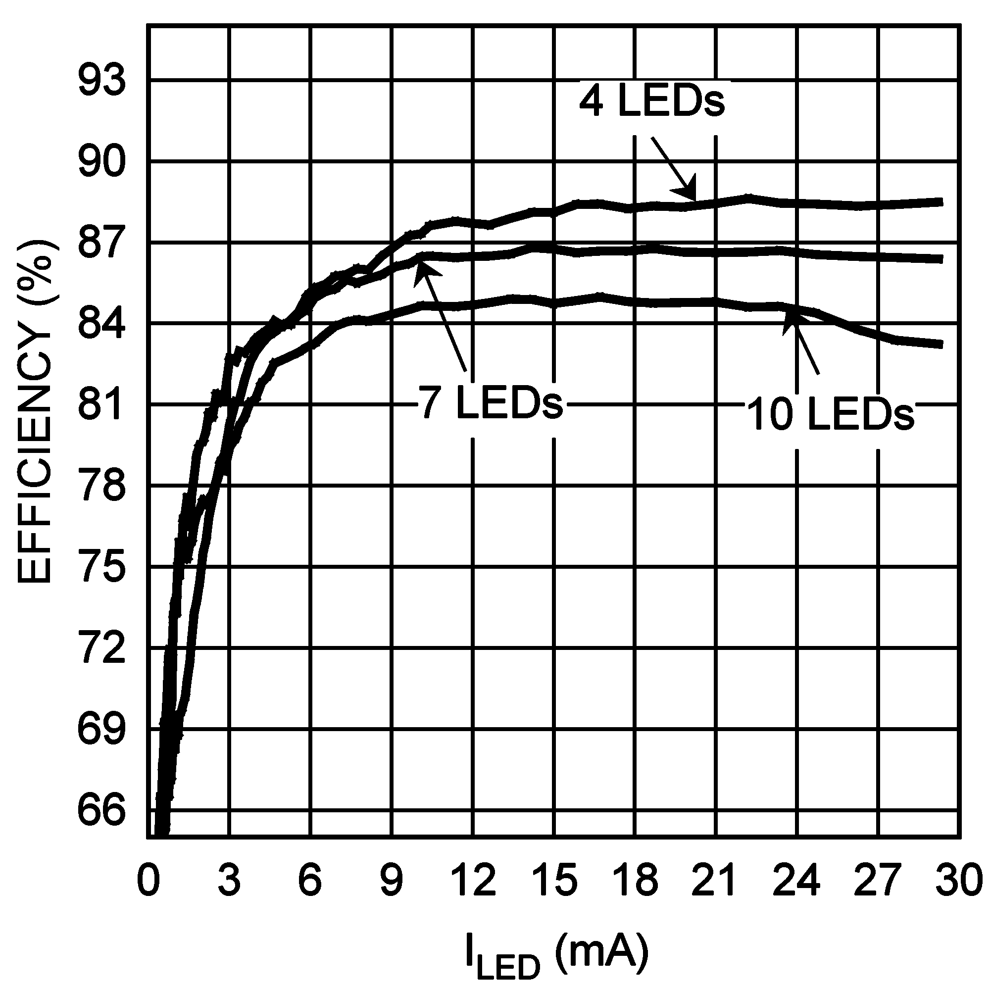
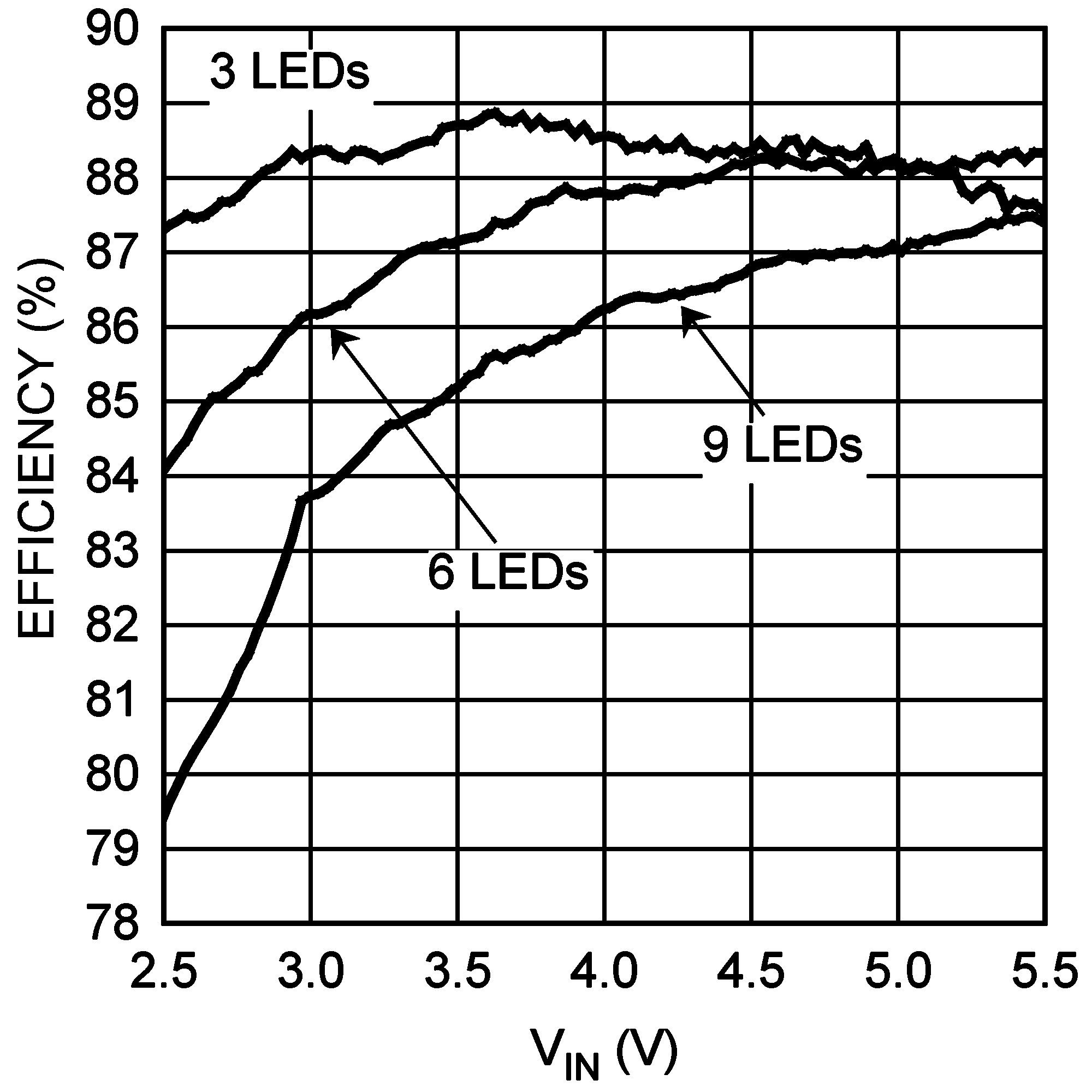
9.2.3 Application Curves
| IFULL_SCALE = 19 mA | ||
| IFULL_SCALE = 19 mA | ||
| IFULL_SCALE = 19 mA | ||